Samsung Expects Huge Chip Performance Gains From Backside Power Delivery
Backside power delivery network (BS PDN) for next-generation chips is a well-known and widely discussed advantage of future process technology. While Intel and TSMC have talked about BSPDN for a while, Samsung only recently shared details about its backside power delivery experiments. It appears the company expects quite noticeable advantages from this innovation.
In a paper presented at the VLSI Symposium in late June, Samsung Electronics reported that the application of a backside power delivery network resulted in a 14.8% reduction in the area of an undisclosed processor compared to the traditional frontside PDN, reports The Elec (via @harukaze5719). Meanwhile, the paper specifically highlighted two Arm circuits, where they observed area reductions of 10.6% and 19%, respectively. A 10% to 19% die area reduction is a major advantage as it enables one to either pack 10% to 19% more transistors and gain performance or reduce the costs of a given chip.
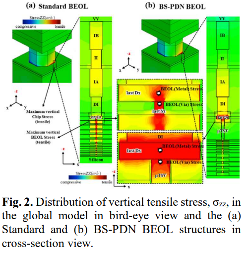
Another thing that Samsung mentioned in its paper was a 9.2% reduction in the wiring length. The backside power rail typically enables thicker wires with lower resistance and, therefore, can drive higher currents for higher performance. A further reduction of wiring length will also bring additional performance advantages.
Additional benefits facilitated by backside power delivery that Samsung revealed were design technology co-optimization knobs that enabled 3.6% Fmax improvement, a 2.4% reduction of standard block area, and 1.6% standard block performance improvement.
Earlier this year, Intel detailed its PowerVia backside power delivery network that will be used for its 20A (2nm-class) fabrication technology and beyond. The benefits of using a backside power rail are widely recognized, and Samsung’s findings prove the theory. Power wires can be made more substantial by shifting power rails to the rear and isolating them from I/O wiring. This thickening reduces resistances in the final production stages, enhancing performance and decreasing energy use. Additionally, this separation leads to a reduced logic area, resulting in cost savings.
Samsung has not disclosed when it plans to implement its BS PDN and with which node. The company is currently polishing off its 2nd Generation 3nm-class gate-all-around transistors-based SF3 fabrication technology and aims to use it for mass production in 2024. The company also has SF3P and 2nm-class SF2 due in 2025. While it is unlikely that Samsung will use a backside power rail for SF3 next year, the company may consider implementing its BS PDN in SF3P or SF2 in 2025.
