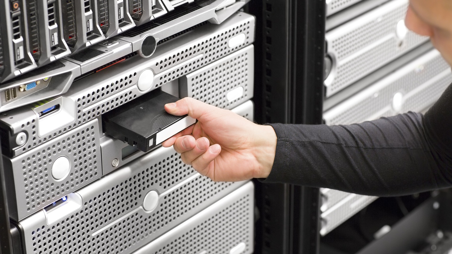
Organizations transitioning cold data storage from hard disks to tape could save a lot of money and cut carbon emissions, according to analysis of various bodies of research by the IEEE Spectrum. The report also cites statements and guidance provided by Brad Johns, an IBM data storage business veteran and data storage consultant.
Research by IDC (PDF, 2019) indicates that 60% of all data would be a good candidate for magnetic tape storage – in other words it would usually be classified as cold data. However, only an estimated 15% of all data is kept on tape. Two key advantages of tape, compared to HDD, are its double lifespan and much lower energy consumption.
The need for data storage is increasing rapidly, with organizations and people commonly generating more, and bigger, files every year. However, research indicates that the files stored by governments, academia, and businesses, as well as busy YouTubers, TikTokers, and Instagrammers, are not necessarily stored in the most efficient way.
We like to look in awe at ultra-modern new-fangled tech solutions for geeky thrills, but sometimes the oldies are goodies. A case in point is in storage technology. We have recently covered breakthroughs in DNA storage, Nanofiche, glass, 5D data cubes and others, but HDDs remain, and optical disks keep re-appearing. Now the idea that magnetic tape should be more prevalent is being pushed forward. However, it looks like HDDs aren’t going extinct despite some companies’ wishful thinking, and tape storage is rolling along quite confidently in the 2020s.
(Image credit: Shutterstock)
According to the IEEE report’s sources, HDDs have a working life of about five years, and produce about 2.55 kg of CO2 per terabyte per year. Compare those figures to the same metrics for tape storage: tape is claimed to have a 30 year lifespan, and produce just 0.07 kg of CO2 per terabyte per year.
The lifespan and CO2 figures show a wide gulf, which organizations can use to their advantage, but it doesn’t end there. Device costs and eWaste statistics also help make the case for cold storage tape systems. In the IEEE report an example is put forward where a data center needs to store 100 petabytes of data for 10 years. Using HDDs would result in 7.4 metric tons of eWaste, but tape storage tech could cut that by more than half, to 3.6 metric tons of eWaste.
Some total cost of ownership (TCO) figures are also put forward to help make the argument for cold storage on tape. Johns calculates that in the 100 PB example, the HDD based data center would have a TCO of $17.7 million over the decade. Meanwhile, the tape storage-based facility could reduce that to about $9.5 million. Money talks.
Companies haven’t been blind to the enduring economic appeal of tape, suggests the source report. However, bigger organizations with more resources have been able to transition better to tape, as correctly classifying and sorting your cold data takes “time, money, and effort,” it is observed.
With momentum seemingly behind its adoption for cold storage, and obvious advantages over HDDs for this data storage model, tape is set to retain a compelling advantage “probably for the next decade,” reckons Johns. That is, unless one of the aforementioned exciting storage breakthroughs ever makes it out of R&D labs.
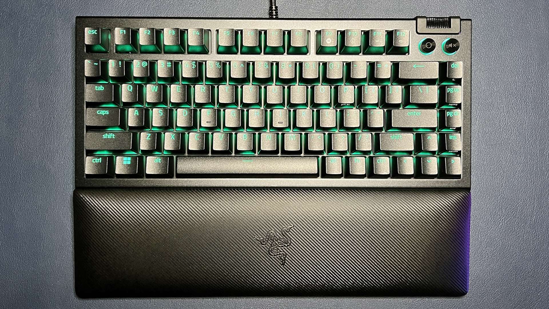
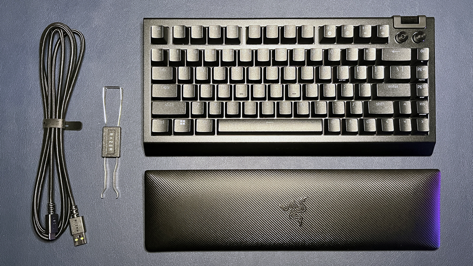
It seems like 2023 is the year gaming companies have decided to get serious about keyboard customizability — physical customizability, that is. The Razer BlackWidow V4 75% may not look like anything out of the ordinary (in fact, it looks almost exactly like a smaller version of the BlackWidow V4 Pro), but this is actually Razer’s first hot-swappable gaming keyboard.
The BlackWidow V4 75% is a wired mechanical gaming keyboard with a compact 75-percent layout and a detachable, padded leatherette wrist rest. For the keyboard enthusiasts it has an aluminum top plate, a hot-swappable PCB, and a gasket-mounted design with two layers of sound-dampening foam, and for the gamers it has N-key rollover, polling rates of up to 8,000 Hz, and bright, customizable per-key RGB (with side underglow).
The BlackWidow V4 75% is available now in black, with Razer’s orange tactile switches, for $189.99. A white version will be released in mid-September, and will cost an extra $10 ($199.99). Razer is also selling standalone 36-packs of its mechanical switches (orange/tactile, green/clicky, yellow/linear) for $24.99 each, but the keyboard will only come with orange switches installed.
Design and Construction of the BlackWidow V4 75%
(Image credit: Tom’s Hardware)
At a glance, the BlackWidow V4 75% looks like a smaller version of the BlackWidow V4 Pro — wrist rest and all. It doesn’t have the V4 Pro’s triple-side underglow, nor does its underglow extend to the wrist rest when connected, but otherwise the new V4 75% shares a very similar overall design, housed in a sturdy black ABS plastic chassis with a matte black aluminum alloy top plate, and machined metal media keys/roller.
Image 1 of 4
(Image credit: Tom’s Hardware)
(Image credit: Tom’s Hardware)
(Image credit: Tom’s Hardware)
(Image credit: Tom’s Hardware)
The BlackWidow V4 75% has a compact 75-percent layout, which is slightly smaller than a TKL layout, with a single column of four navigation keys (versus the TKL’s three-column, two-row cluster of six). While many 75-percent keyboards leave some space between the main keys, arrow keys, and navigation keys, the V4 75% does not — the navigation keys and arrow keys are right next to the main keys. This shaves off a few millimeters from the keyboard’s overall length: the BlackWidow V4 75% measures 12.6 inches (321mm) long, versus Asus ROG Azoth’s length of 12.83 inches (326mm). It’s a bit wider than other keyboards — 6.1 inches (155.5mm), thanks to a slope at the bottom that allows the wrist rest to nestle up against it.
Image 1 of 4
(Image credit: Tom’s Hardware)
(Image credit: Tom’s Hardware)
(Image credit: Tom’s Hardware)
(Image credit: Tom’s Hardware)
It’s sturdily constructed but not overly heavy, weighting 1.8lbs (815g) — not nearly as heavy as the Azoth (2.61lbs / 1186g), but a little heavier than the SteelSeries Apex Pro TKL Wireless (1.65lbs / 747g). On the bottom, you’ll find four rubber non-slip grips and two sets of flip-out feet, which add an extra 6 degrees or 9 degrees of height to the back of the keyboard.
Razer BlackWidow V4 Pro (Image credit: Tom’s Hardware)
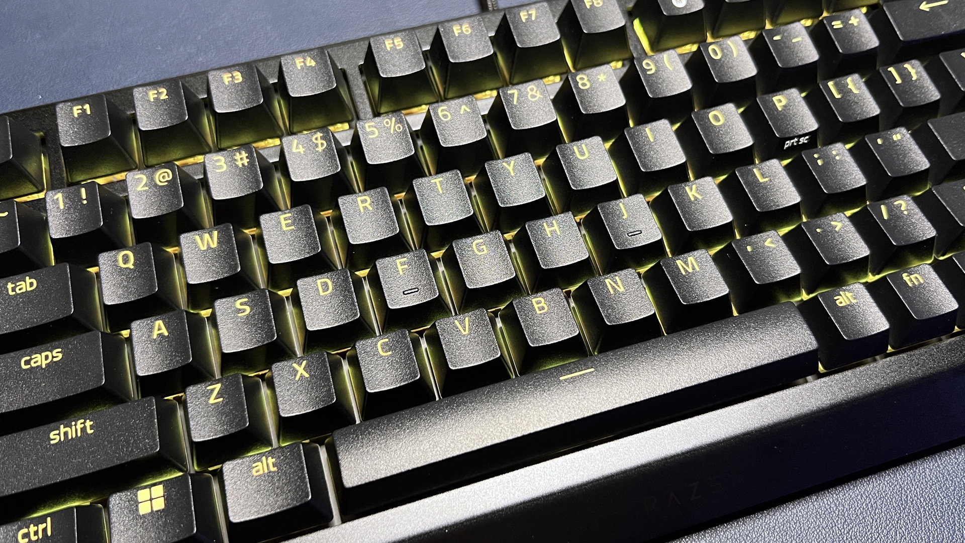
The BlackWidow V4 75% comes with Razer’s doubleshot ABS keycaps, which are full-height, lightly textured, and have shine-through primary legends and printed (white) secondary legends. While I had no issues with the keycaps in my testing, I’ve found that Razer’s ABS keycaps tend to start showing wear within the first few months of use.
I’ve been using the BlackWidow V4 Pro intermittently since it launched six months ago, and several of the keycaps are already shiny from wear. While shininess is something that tends to come pretty quickly on ABS keycaps, it seems to come quicker on Razer’s.
Image 1 of 2
(Image credit: Tom’s Hardware)
(Image credit: Tom’s Hardware)
In the upper right corner, the BlackWidow V4 75% features a volume roller and two media keys, all made of machined metal. Interestingly, the right media key, which has a mute symbol etched into it, can be reprogrammed using Razer’s Synapse 3 software. But the left media key, which has a generic circle etched into it, cannot be reprogrammed — this media key is set to play/pause on a single tap, skip to the next track on a double-tap, and go back to the previous track on a triple-tap.
Image 1 of 3
(Image credit: Tom’s Hardware)
(Image credit: Tom’s Hardware)
(Image credit: Tom’s Hardware)
The BlackWidow V4 75% comes with a detachable magnetic leatherette wrist rest, which is padded and has a woven-textured surface. The wrist rest looks like a smaller version of the one that comes with the BlackWidow V4 Pro, but simpler — it doesn’t have a connection point to transfer the keyboard’s underglow, because the V4 75% doesn’t have full underglow (it has underglow on either side, but not along the bottom).
(Image credit: Tom’s Hardware)
Also in the box: a 6.5-foot (2m) detachable USB-C to USB-A cable, and a combination keycap/switch puller.
Specs
Swipe to scroll horizontally
Switches
Razer Orange (Linear)
Lighting
Per-key RGB, underglow (sides)
Onboard Storage
Yes (5 profiles)
Media Keys
Yes, volume roller
Game Mode
Yes
Connectivity
USB-C
Additional Ports
0
Keycaps
Double-shot ABS
Construction
Aluminum top plate
Software
Synapse 3
Dimensions (LxWxH)
12.6 x 6.1 x 0.94 inches / 321 x 155.5 x 24mm
Weight
1.8lbs / 815g
MSRP / Price at Time of Review
$179.99 / $179.99
Release Date
Aug. 17, 2023
Typing and Gaming Experience on the BlackWidow V4 75%
The BlackWidow V4 75% is a wired 75-percent gaming keyboard with N-key rollover, a polling rate of up to 8,000 Hz, and Razer’s third-gen orange tactile mechanical switches. In a bid to appeal to the keyboard enthusiast side of gamers, the V4 75% also features a tape-enhanced hot-swappable PCB (which accepts both 3- and 5-pin switches) and a gasket-mounted design with two layers of dampening foam.
Image 1 of 3
(Image credit: Tom’s Hardware)
(Image credit: Tom’s Hardware)
(Image credit: Tom’s Hardware)
The BlackWidow V4 75% comes with Razer’s third-gen orange tactile mechanical switches, which have an actuation force of 50g, an actuation point of 2mm, and a full travel distance of 3.5mm. These switches have a mild tactile bump but are relatively quiet otherwise, and feel similar to Cherry MX Brown switches — albeit slightly heavier, as the MX Browns have an actuation force of 45g. Razer’s switches are rated for 100 million keystrokes and have a box-style cross stem that’s compatible with most third-party keycaps.
Typing on the BlackWidow V4 75% felt and sounded better than expected — especially if you’re coming from a mainstream gaming keyboard (such as any of Razer’s previous keyboards). The tactile switches combined with the gasket-mounted FR4 plate made for a springy-but-quiet typing experience, even if Razer’s orange switches (and all of Razer’s switches) are slightly stiffer than I prefer. The V4 75% and the V4 Pro sound vastly different — and the V4 Pro doesn’t sound terrible, but you can absolutely hear the tape-modding and sound-dampening foam at work in the V4 75%.
(Image credit: Tom’s Hardware)
That said, is it the best-sounding keyboard I’ve used recently? Not exactly. I definitely noticed some stabilizer rattle — not in the spacebar, so much, but in the enter and backspace keys — despite the V4 75%’s factory-lubed, plate-mounted stabilizers. But that’s pretty nit-picky; overall, the V4 75% sounds better than 99% of mainstream gaming keyboards on the market.
As for gaming, the BlackWidow V4 75% performed — as expected — very well, with no latency or lag, though the orange switches’ tactile bump and slightly-heavier actuation force may start to fatigue your fingers if you’re used to smooth, lightweight linear optical switches.
The keyboard has a default polling rate of 1,000 Hz, but you can bump this up to 8,000 Hz in Razer’s Synapse 3 software. This is a wired keyboard so there’s no concern about a higher polling rate eating up battery life, but it does use more processing power and Razer warns that an 8,000 Hz polling rate “may result in reduced frame rate when playing CPU bound games.” I didn’t notice any reduced frame rates in my testing, and I’ve mostly been playing Baldur’s Gate 3, which is CPU-heavy.
Features and Software of the BlackWidow V4 75%
The BlackWidow V4 75% works well out of the box, but can be configured using Razer’s Synapse 3 software. While anyone who knows me knows that I hate Synapse 3, I didn’t hate it quite as much this time — probably because there’s not quite as much to customize on this keyboard.
Image 1 of 2
(Image credit: Tom’s Hardware)
(Image credit: Tom’s Hardware)
You can use Synapse 3 to remap keys (two layers, thanks to Razer’s “HyperShift” duplication tech), adjust the polling rate, and configure the keyboard’s per-key RGB and side underglow, either with preset quick effects or using Razer’s unnecessarily advanced Chroma Studio. As I mentioned earlier, the media keys are sort of programmable — you can program the roller (up/down) and the mute key (single press only), but you cannot program the play/pause key.
It’s a little strange that you can’t at least program the same number of layers for the mute key as exist on the play/pause key, but perhaps Razer will update that in one of its future hourly Synapse 3 updates.
The Bottom Line
The BlackWidow V4 75% is a pretty solid offering for Razer’s first hot-swappable keyboard, but it’s far from perfect. I’m a little disappointed that it looks so… boring, considering it’s Razer’s foray into a new category — the chunky black on black on black just isn’t doing it for me. Also, while it is fairly (physically) customizable once you get your hands on it, it’s disappointing that it’s not being offered with different switch options, or with different keycap options (Razer doesn’t make its PCB keycaps in a 75-percent layout and doesn’t plan to at the moment), and that the white version is more expensive (I know it’s only $10, but still).
But for $189.99, it’s one of the better-sounding gaming keyboards you’ll find. I’m personally a bigger fan of the Asus ROG Strix Scope II 96 Wireless’ (also $179.99) sound, but if you’re looking for something smaller than an almost-full-size keyboard, the BlackWidow V4 75% is a good choice.
MORE: Best Gaming Keyboards
MORE: How to Pick Keycaps for Your Mechanical Keyboard
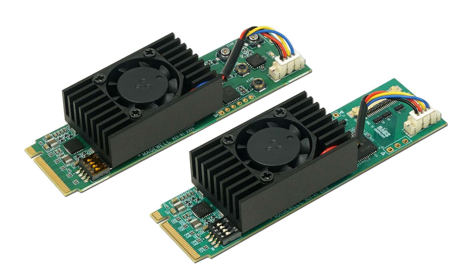
Capture card manufacturer Magewell has unveiled two new highly-capable 4K capture cards sporting a highly unusual M.2 form factor. The new card’s are known as the Eco Capture HDMI 4K Plus M.2 and Eco Capture 12G SDI 4K Plus M.2. As the names suggest, one model is designed to work with HDMI connectors while the other is designed to work with SDI ports, which is a video connector used by the professional video production industry.
M.2 capture cards are not something you often hear about, but the ultra-compact form factor has many advantages. One of the biggest advantages is integration with newer motherboards that sacrifice most of their smaller PCie x8, x4, and x1 slots for M.2 slots. In these cases, having an M.2 capture card instead of a traditional half-height or full-height PCIe card can be really effective, especially if a system is already using the remaining one or two standard PCIe slots for graphics cards, audio cards, and/or ethernet cards.
Another use is with Mini-ITX motherboards which have even fewer PCIe slots than ATX and micro-ATX motherboards. In cases where the primary and only PCIe x16 slot is being used, M.2 is the only way to add additional PCIe devices to the system. Lots of Mini-ITX boards have more than one M.2 slot as well, which will allow users to build a full Mini-ITX system without sacrificing M.2 storage.
With these capture cards, streamers, video enthusiasts, and professionals can re-route all their video encoding and video processing to the capture card. This offloads work from the CPU and GPU, freeing up resources and improving image quality in some cases (depending on how slow or old the CPU or GPU is). Most people will find the built-in encoders found in the best GPUs and best CPUs to be more than adequate. But, a dedicated capture card can still be beneficial for highly-demanding setups that require more processing power than what a built-in CPU/GPU encoder can provide.
The M.2 card’s themselves come in a 22 x 80 mm form factor, similar to that of 2280-sized M.2 SSDs. Both cards come with a green PCB and feature a large black cooling solution on top, with a very tiny fan actively cooling the encoding chip underneath. Since the M.2 standard does not feature any external ports, the cards need to be used with a special adapter that connects the card to a full-sized HDMI or SDI connector.
According to Magewell, these two new cards offer double the frame rate of their previous versions, featuring 60FPS playback at resolutions of up to 4096×2160 (ie. 4K resolution). Both cards are compatible with Windows and Linux operating systems and support native video APIs like DirectShow, DirectKS, V4L2, and ALSA. Plus, they also support high-quality upscaling, downscaling, cross-scaling, and color space conversion.
Pricing has not been unveiled just yet, but the Eco Capture HDMI 4K Plus M.2 is reportedly now shipping, and the Eco Capture 12G SDI 4K Plus M.2 will be available in the next two months.
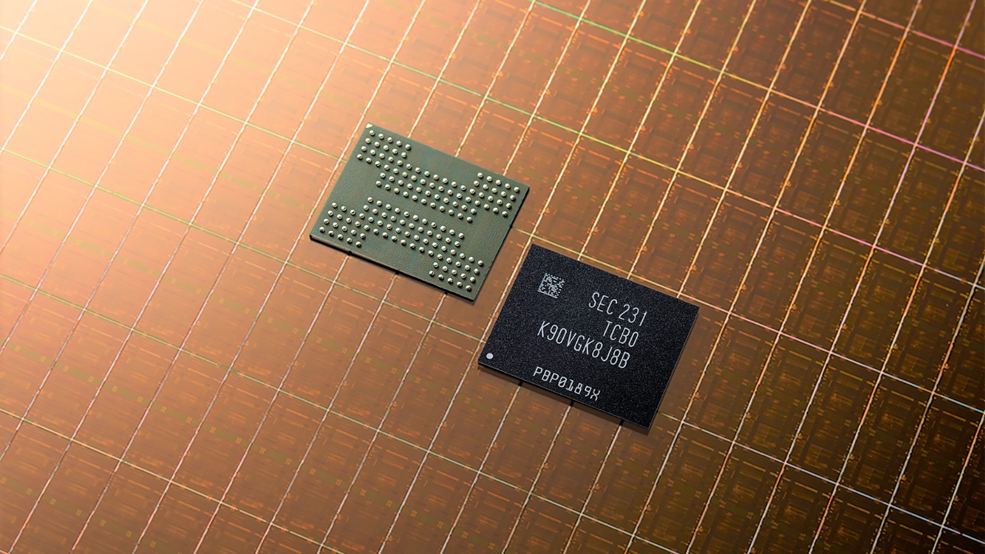
Samsung Electronics is poised to employ double-stack architecture for its 9th Generation 3D-NAND memory when it starts its production next year, according to a DigiTimes report that cites Seoul Economic Daily. The sets Samsung apart from SK Hynix, which uses three stacks of NAND to build its 321-layer 3D NAND devices when they enter mass production in the first half of 2025.
Samsung’s 9th Generation V-NAND with over 300-layers is set to hinge on the double-stack technique, which Samsung first embraced in 2020 with its 7th generation 176-layer 3D NAND chips. This method involves production of one 3D NAND stack on a 300 mm wafer and then building another stack on top of the first one. Samsung’s 300-layer 3D NAND will increase storage density produced on one wafer and will enable makers to build lower-cost SSDs or make the best SSDs cheaper.
Contrarily, rival SK Hynix has revealed its intent to kick off the production of its 321-layer 3D NAND in 2025 using a triple-stack approach. This procedure, distinct from Samsung’s, will involve creating three distinct sets of 3D NAND layers, which will increase the number of steps and usage of raw materials, but is meant to maximize yields as it is easier to produce 3D NAND stacks with fewer layers.
Industry speculations that rely on leaked roadmaps suggest that post their 9th Generation 3D NAND, Samsung might adopt a triple-stack methodology for its 10th generation 430-layer 3D NAND. Some experts told Seoul Economic Daily that surpassing 400 layers in 3D NAND would necessitate usage of three separate stacks of 3D NAND, possibly due to yields concerns. Meanwhile, this will naturally increase usage of raw materials and increase costs per 3D NAND wafer.
Samsung’s long-term vision, as presented at the Samsung Tech Day 2022 last October, aspires to reach up to 1,000 layers by 2030.
Nvidia is raking in up to 1,000% in profit for each H100 GPU accelerator it sells, according to estimates made in a recent social media post from Barron’s senior writer Tae Kim. In dollar terms, that means that Nvidia’s street-price of around $25,000 to $30,000 for each of these High Performance Computing (HPC) accelerators (for the least-expensive PCIe version) more than covers the estimated $3,320 cost per chip and peripheral (in-board) components. As surfers will tell you, there’s nothing quite like riding a wave with zero other boards on sight.
Kim cites the $3,320 estimated cost for each H100 chip as coming from financial consulting firm Raymond James. It’s unclear how deep that cost analysis goes, however: if it’s a matter of pure manufacturing cost (averaging the price-per-wafer and other components while taking yields into account), then there’s still a significant expense margin for Nvidia to cover with each of its sales.
Product development takes time and resources; and considering the engineers and other participants within the product development lifecycle for a product such as H100, Nvidia’s R&D costs also have to be taken into account before a final, average product development cost can be reached. According to Glassdoor, Nvidia’s average salary for an electronics hardware engineer sits at around $202,000 per year. And that’s for a single engineer – it’s likely development of chips such as the H100 require thousands of hours from a number of specialized workers. All of that too has to be taken into account.
Even so, it can’t be denied that there are advantages at being the poster company for AI acceleration workloads. By all accounts, Nvidia GPUs are flying off the shelves without even getting personal with the racks they’re piled on. This article in particular looks to be the ultimate playground for anyone trying to understand exactly what the logistics behind the AI HPC boom means. What that actually translates to, however, is that it seems that orders for Nvidia’s AI-accelerating products are already sold through until 2024. And with expectations of the AI accelerator market being worth around $150 billion by 2027, there’s seemingly nothing else in the future but green.
And of course, that boom is better for some than others: due to the exploding interest in AI servers compared to more traditional HPC installations, DDR5 manufacturers have had to revise their expectations on how much the new memory products will penetrate the market. It’s now expected that DDR5 adoption will only hit parity with DDR4 by 3Q 2024.
The company is reaping the benefits of having built its infrastructure and product stack on the back of its tooling and bets on AI as the next big thing.
But budgets everywhere tend to have limits, and there’s also the matter of opportunity cost: investing into AI acceleration at its current prices will lock some players’ doors to investments in other spaces, or limit how much risks they can take in pursuing less-safe research and development venues.
When all is said and done, Nvidia’s bottom line as buoyed by its AI chip sales could now cover inane amounts of leather jackets. At least from that perspective, Nvidia CEO Jensen Huang has to be beaming left and right.
Entry-level builds, even budget builds, have crept up in price. Often times, despite paying $1,000 or more, you can still wind up with something that feels cheap. That’s not the case with the Maingear MG-1 Silver ($1,149 to start, $1,249 as tested), a desktop that feels premium, even if it has the performance of a starter rig.
The Intel Core i5-13400F and Nvidia GeForce RTX 4060 don’t have the power of some of the best gaming PCs, but the system plays games well enough, especially if you’re willing to adjust settings. We only found one component – the SSD – to be subpar. But that’s replaceable, or at least can be augmented with another one down the line.
But most importantly, you still get a fairly premium chassis, meticulous cable management, and a sense that this is a computer you can grow with. When you’re ready to spend more or learn to upgrade yourself, this case has nothing proprietary, and it will be able to grow with you.
Design of the Maingear MG-1 Silver
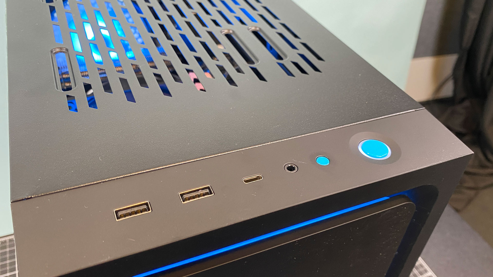
Maingear’s MG-1 Silver is, in many ways, a classic mid-tower, though it’s compact enough to fit on most desks. The chassis is a black aluminum box with a window on the left side panel to let you see your parts and RGB lighting. The blue power and LED buttons on top serve as small accents that you won’t see much.
Image 1 of 3
(Image credit: Tom’s Hardware)
(Image credit: Tom’s Hardware)
(Image credit: Tom’s Hardware)
At 19 x 16.88 x 8.13 inches, the Maingear MG-1 is fairly compact. The Alienware Aurora R16, newly redesigned to be a more conventional size, is 18.05 x 16.5 x 7.76 inches, which is slightly smaller.
The faceplate on the front of the Maingear system attaches magnetically and can easily be pulled off and reattached. A small connector on the bottom of the faceplate provides power to RGB lighting behind the faceplate (which creates a glowing effect around it) and in the Maingear logo). Our review unit is Maingear’s “Shroud Edition,” named after the pro esports player and streamer, so it included a black front panel with Shroud’s logo on it. It also included a limited time “Into the Wild” faceplate based on his latest fashion line. But you can also design your own faceplate ($99 each), and Maingear tossed one it made in our box, which featured a magical space theme and the Tom’s Hardware logo.
Image 1 of 3
(Image credit: Tom’s Hardware)
(Image credit: Tom’s Hardware)
(Image credit: Tom’s Hardware)
That front panel sits in front of three 120 mm intake fans, while another fan in the back exhausts heat from the case. Our unit featured a Cooler Master Hyper 212 air cooler, but there is room in the top of the chassis for up to a 360 mm radiator for an all-in-one cooler in more expensive configurations. Regardless of the lack of fans up top, I wish there were some sort of dust filter in place. In fact, I wouldn’t mind seeing dust filters by the front intake fans, either. (The only one I spotted was underneath the power supply).
Maingear’s RGB is powered by a controller mounted on the right side of the case, and can be adjusted with a remote control. While this let me change colors, brightness, and patterns, it only adjusted the rear fan and a lightstrip. The other parts with RGB, like the RAM, didn’t work with the remote, however. That led me to install MSI Center with its Mystic Light add-on for lighting control. While our motherboard doesn’t have lighting, it can control the RAM and let me match it to the rest of the system. (And it takes a lot to make me want to use MSI Center!).
While our review unit came with a micro-ATX motherboard, there’s room in the system for a larger, full-sized ATX board.
2x USB 3.2 Gen 1 Type-A, USB 3.2 Gen 2 Type-C, 3.5 mm headphone jack, RGB LED button
Rear Ports (Motherboard)
USB 3.2 Gen 2 Type-A, USB 3.2 Gen 2 Type-C, 4x USB 3.2 Gen 1 Type-A, 2x USB 2.0, Ethernet, HDMI, audio connectors
Video Output (GPU)
HDMI, 3x DisplayPort
Power Supply
600W EVGA B
Cooling
Cooler Master Hyper 212 air cooler, 4x 120mm case fans
Operating System
Windows 11 Home
Dimensions
19 x 16.88 x 8.13 inches
Other
Shroud front panel, “Into the Wild” front panel
Price as Configured
$1,249
Ports and Upgradeability on the Maingear MG-1 Silver
On the front panel, there’s a pair of USB 3.2 Gen 1 Type-A ports and a USB 3.2 Gen 2 Type-C port, as well as a 3.5 mm headphone/mic jack. There’s also a dedicated button for switching between RGB states next to the power button.
(Image credit: Tom’s Hardware)
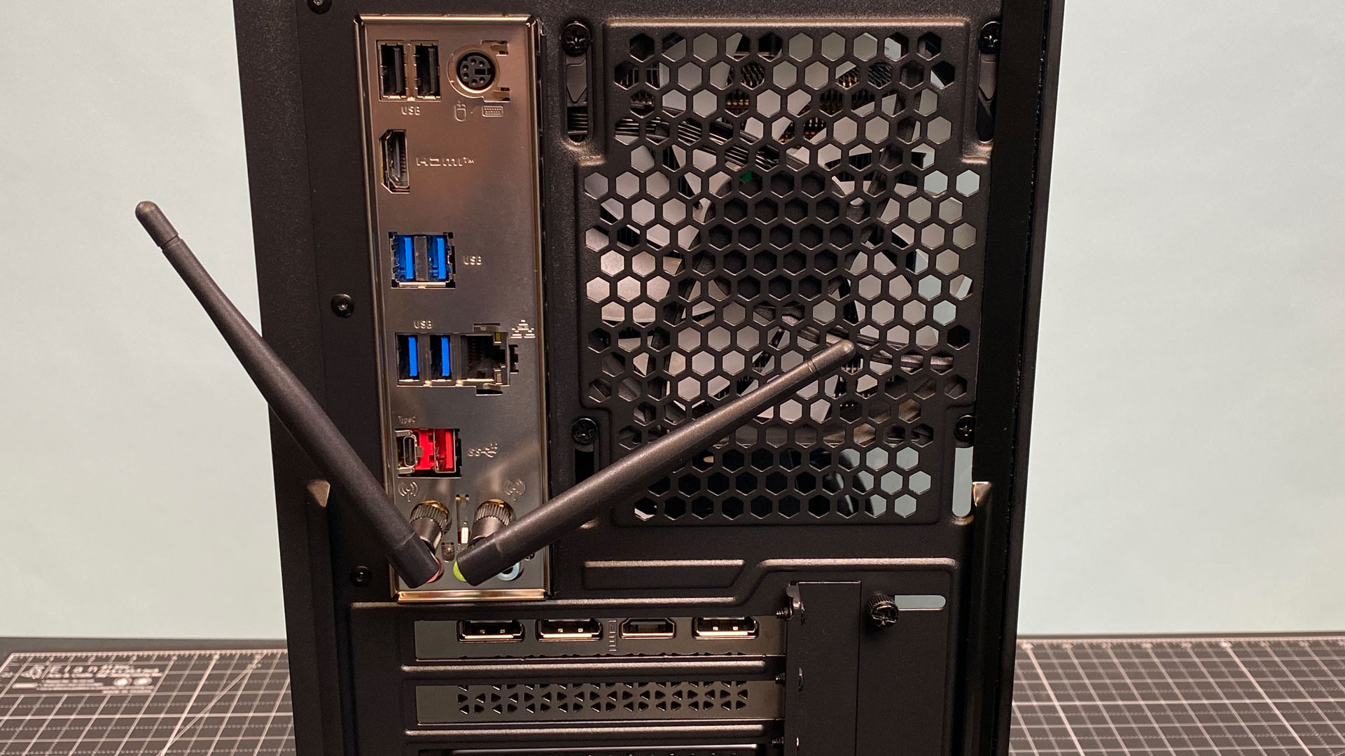
The back panel will depend on which motherboard you get. On the rear of the MSI PRO B660M-A CEC WiFi DDR4 in our review unit, that meant USB 3.2 Gen 2 Type-A, USB 3.2 Gen 2 Type-C, four USB 3.2 Gen 1 Type-A, ports, two USB 2.0 ports, Ethernet, HDMI, and audio connectors.
(Image credit: Tom’s Hardware)
For video, that also depends on the GPU. The RTX 4060 in the Silver we tested has a single HDMI port and four DisplayPort connectors.
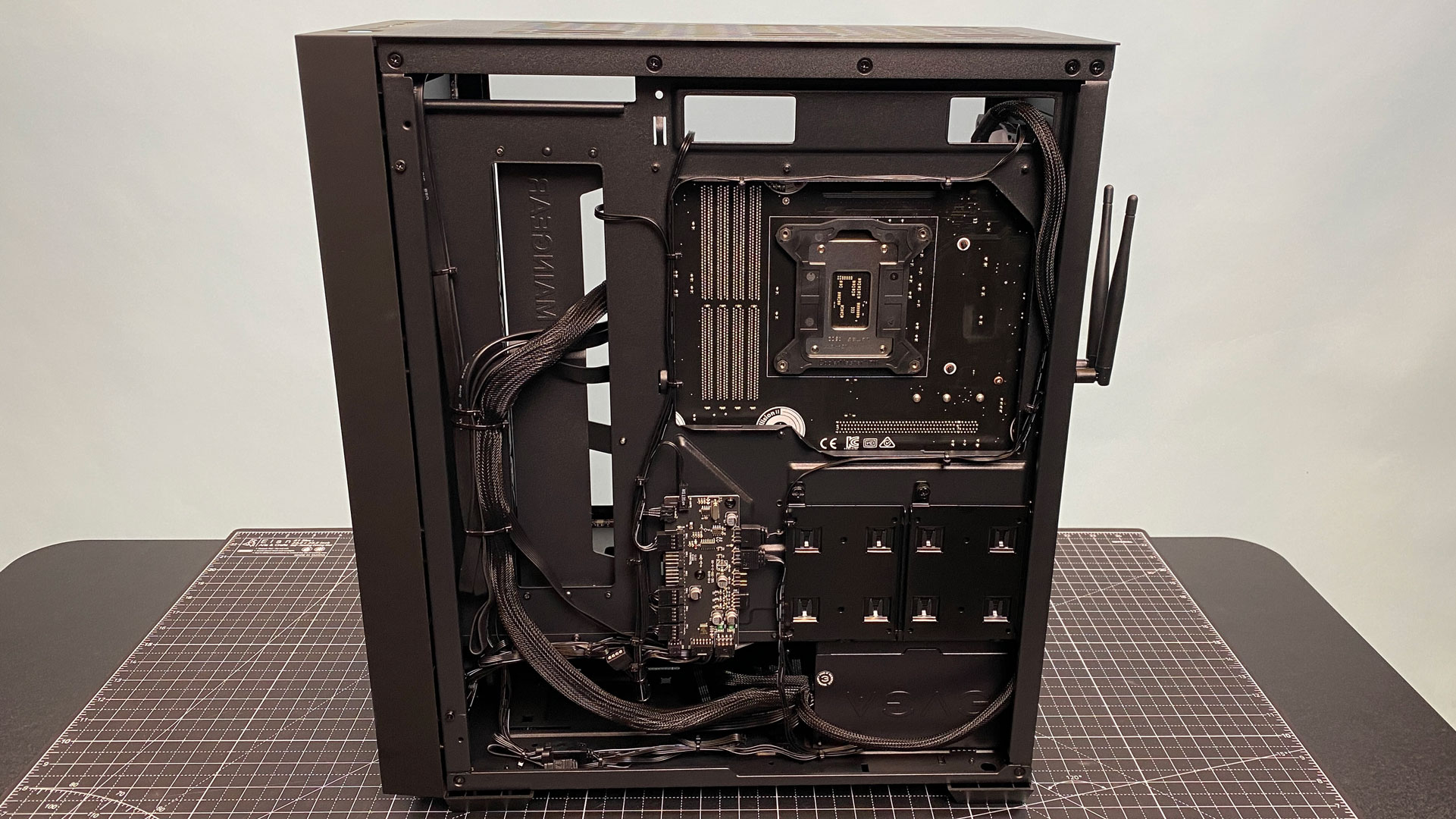
Opening the MG-1 is simple. The left side panel, with the glass window, is held on by two thumb screws. With those removed, it just slides off. It’s the same for the right side panel, but the entire side comes off there. Cable management is all neat and tidy; whoever built this had more patience than I do. Some of that has to do with the RGB and fan controller in the back of the system, with much of the cable mess tied and connected there, rather than in front of the motherboard.
(Image credit: Tom’s Hardware)
When you’re in, upgrading the MG-1 is much like changing parts on anything you’ve built yourself. There’s nothing proprietary here. That means you have full access to the motherboard, cooler, fans, RAM, CPU, GPU, power supply, or anything else you’d want to change within the case. Some quick upgrades you could make in our review unit include adding a second SSD (there’s another slot on our motherboard and mounts on the back for SATA drives, though with the way the power and data cables are tied up, you may have a hard time getting them hooked up) or adding more RAM. Eventually, you could replace the entire motherboard if you wanted to switch CPU platforms.
Gaming and Graphics on the Maingear MG-1 Silver
Most companies that lend gaming PCs for review don’t send the low-end configuration (presumably, they want to only be affiliated with the most powerful options). So when Maingear sent the MG-1 Silver with an Intel Core i5-13400F, 16GB of RAM, a GeForce RTX 4060 and 512GB m.2 NVMe SSD, we had a limited test pool for comparison. So here, we’re comparing it to the recently reviewed Alienware Aurora R16, with a Core i7-13700F, 32GB of DDR5 RAM and an RTX 4070. It’s not exactly competition, but shows what you can get if you have an extra $600 to spend.
I used the Maingear to play Returnal, and while the game suggested low settings, it did decently on the high preset, even at 4K. With that combination of graphics settings and resolution, it still ran between 48 and 59 frames per second in early areas of the game, hitting the lower ranges in combat with aliens.
Image 1 of 5
(Image credit: Tom’s Hardware)
(Image credit: Tom’s Hardware)
(Image credit: Tom’s Hardware)
(Image credit: Tom’s Hardware)
(Image credit: Tom’s Hardware)
If you have a high refresh rate monitor, you may want to turn down some settings, but the MG-1 Silver performed decently in our benchmarks.
On Shadow of the Tomb Raider (highest settings), the Maingear hit 104 fps at 1080p and eked out 30 fps at 4K.
When it came to Grand Theft Auto V (very high), the game hit 95 fps at 1080p and 28 fps at 4K.
Far Cry 6 (ultra) was the Maingear’s best attempt at 4K, hitting 38 fps, but you might be more comfortable with the 91 fps at 1080p.
Red Dead Redemption 2, at medium settings, is still a challenge for many computer. The Maingear reached 71 fps at 1080p, but an unplayable 21 fps at 4K.
On Borderlands 3 (badass preset), the Maingear reached 104 fps at 1080p and a flat 30 fps at 4K.
To stress test systems, we run the Metro Exodus benchmark at RTX settings at 1080p for 15 runs, simulating about half an hour of game play. The Maingear achieved an average frame rate of 57 fps and was largely consistent within a few decimal points throughout the tests. The CPU’s six performance cores averaged 3.33 GHz, while the four efficiency cores ran at 2.62 GHz. The CPU package measured 43.1 degrees Celsius. The GPU ran at 1.9 GHz and measured 53.55 degrees Celsius.
Productivity Performance
Many people use their gaming PCs as productivity machines as well. The Intel Core i5-13400F and RTX 4060 in the Maingear rig should be plenty for most everyday tasks, though the SSD leaves something to be desired. It’s unsurprising that the Maingear lost out to the Alienware Aurora in these tests, with its more powerful 13th Gen Core i7, but it’s also a more expensive machine.
Image 1 of 3
(Image credit: Tom’s Hardware)
(Image credit: Tom’s Hardware)
(Image credit: Tom’s Hardware)
On Geekbench 6, a CPU-heavy synthetic benchmark, the MG-1 Silver earned a single-core score of 2,330 and a multi-core score of 9,743. The difference in single-core between the MG-1 and the Alienware wasn’t bad, but the i7, with more cores, reached 16,687 points.
The big negative for the Maingear rig was on our file transfer test. The MG-1’s 512GB Solidigm P41 Plus copied 25GB of files at 489.65 MBps, which is slower than our hopes for any PC these days. When we reviewed that drive, we said it had “largely mediocre performance.”
When we used Handbrake to transcode a 4K video to 1080p, it took the MG-1 and its Core i5 5 minutes and 24 seconds to complete the task. The more powerful, pricier Alienware did it in 3:52.
Software and Warranty on the Maingear MG-1 Silver
For better or worse, our Maingear MG-1 Silver review unit came without much software preinstalled, other than what you need for the Nvidia GPU. I do wish the RGB controller had some software. If I wanted something for any of the components, I’d need to add it myself.
That being said, there’s really no bloatware. The only real junk comes from the Windows 11 side of things, including links in the start menu to install apps like Whatsapp, Netflix, Prime Video, Messenger, and Instagram.
By default, Maingear includes a 1-year warranty and “lifetime support.” You can upgrade to a 2 or 3-year warranty for $99 and $199, respectively.
Maingear MG-1 Silver Configurations
Maingear offers its MG-1 with a wide variety of configuration options, as well as a series of pre-built, ready-to-ship configs.
We tested the Maingear MG-1 Silver Shroud Edition, with an Intel Core i5-13400F,
MSI PRO B660M-A CEC WiFi DDR4 motherboard, 16GB of RAM, a
GeForce RTX 4060 and 512GB Solidigm P41 Plus m.2 NVMe SSD. The Shroud Edition moniker adds the eponymous esports player and streamer’s logo to the front panel and also includes a secondary front panel matching his latest clothing collection. All of that will cost you $1,249.
If you ditch the Shroud Edition for the regular MG-1 Silver, you’ll get the exact same PC, but without Shroud’s logo or the extra faceplate. That will save you $100 at $1,149, making it the one I would get.
There are numerous other options, including Gold (bumps up to an RTX 4060 Ti, $1,299 for standard, $1,399 for Shroud edition) up through the most expensive Ultimate edition (a Core i9-13900K, RTX 4090, 32GB DDR5 RAM, 2TB SSD, a 1,000W PSU, and a 360mm AIO liquid cooler) which starts at $4,599 (or $4,699 for the Shroud edition).
Mangear also sent an extra faceplate featuring the Tom’s Hardware logo with our loaner. That customized front panel costs $99, should you want to add your own look.
Bottom Line
For those who are just getting into PC gaming, or don’t have the budget to splurge on the top of the line, the Maingear MG-1 Silver is impressive. Sure, it doesn’t have all of the power, bells and whistles that PC gaming can offer, but it’s also less than $1,500. And because the design hsa no proprietary parts like some computer makers use, you have the ability to upgrade everything you want in this case in the future. You could bump up, either through Maingear’s own options or for something like the Alienware Aurora R16, but those upgrades raise the price pretty quick.
One note on price: I don’t know who the Shroud edition is for. Unless you’re a superfan of Shroud, as either a streamer or esports pro, I don’t know why you’d want special edition Shroud faceplates that add $100 to the cost. Especially when you can submit your own design for the same price. Me? I’d rather have that money for games, or a faster, roomier SSD.
The cable management is meticulous, perhaps too much so (you’ll want to get a power cable out eventually), and Maingear could add a few dust filters to the system in order to keep things cleaner in the long run. But despite being a fairly cheap gaming system, outside of a sluggish SSD, the Maingear MG-1 Silver never feels like one.
When Intel announced major workforce cuts to certain divisions in October, 2022, it was considered a drastic move. But apparently, it was not enough, which is why in May, 2023 the company initiated another round of layoffs in its client computing group (CCG) and its data center group (DCG). Apparently, the company is now cutting its research and development personnel in California, according to a Sacramento Inno report.
Intel is laying off 140 employees in California: 89 employees are being let go at Intel’s Folsom campus and 51 jobs will be cut in San Jose. There are 37 job classifications affected at the Folsom site, the primary titles among the affected positions are ‘engineer’ and ‘architect,’ the report claims. Specifically, Intel is laying off 10 GPU software development engineers, eight system software development engineers, six cloud software engineers, six product marketing engineers, and six system-on-chip design engineers.
This latest reduction marks nearly 500 positions removed from the Folsom R&D campus in the current year, following previous cuts in January, March, and May. As of early 2022, Intel had 5,300 employees in Folsom.
Intel’s Folsom campus has been used for a variety of R&D activities, including development of SSDs, graphics processors, software, and even chipsets. Since Intel got rid of its 3D NAND and SSD division in 2021, by now it has either transferred appropriate specialists to Solidigm, or let them go. As a result, it is now laying off its GPU specialists, which is a bit surprising as the company’s GPU software is far from perfect. Perhaps, the company wants to move certain positions to other locations with cheaper workforce, but Intel has yet to comment on the matter.
In correspondence with state officials, Intel mentioned the possibility of relocating affected employees within the company. A spokesman for Intel also noted that Intel retains over 13,000 staff in California and remains committed to investing in fundamental areas of its business, notably its manufacturing operations within the U.S. Meanwhile, the majority of Intel’s U.S. production takes place in Arizona, Oregon, and New Mexico.
Whether you want to record some footage off of a games console or stream from a dedicated streaming PC the Elgato 4K60 pro could be your answer. Currently, you can save a whopping $50 off of the price of this capture card and pick up the Elgato 4K60 pro for $199 on Amazon. This is the mark-2 variant and features a low latency 240Hz passthrough to make your streams and recordings as smooth as possible.
A great price for a QHD 32-Inch monitor sees the LG UltraGear 32GN600-B gaming monitor on sale at Walmart for $209. A fast 165Hz refresh rate, good color representation, HDR10, and AMD FreeSync integration help this monitor to be a decent option for a well-priced main gaming monitor.
Not too large at just 28 inches the 4K Gigabyte M28U is reduced by $100 to only $429 at Newegg. With great pixel density thanks to its size, and a speedy 144Hz refresh rate, this monitor also sports HDMI 2.1 support, and a KVM switch for easily connecting to different devices.
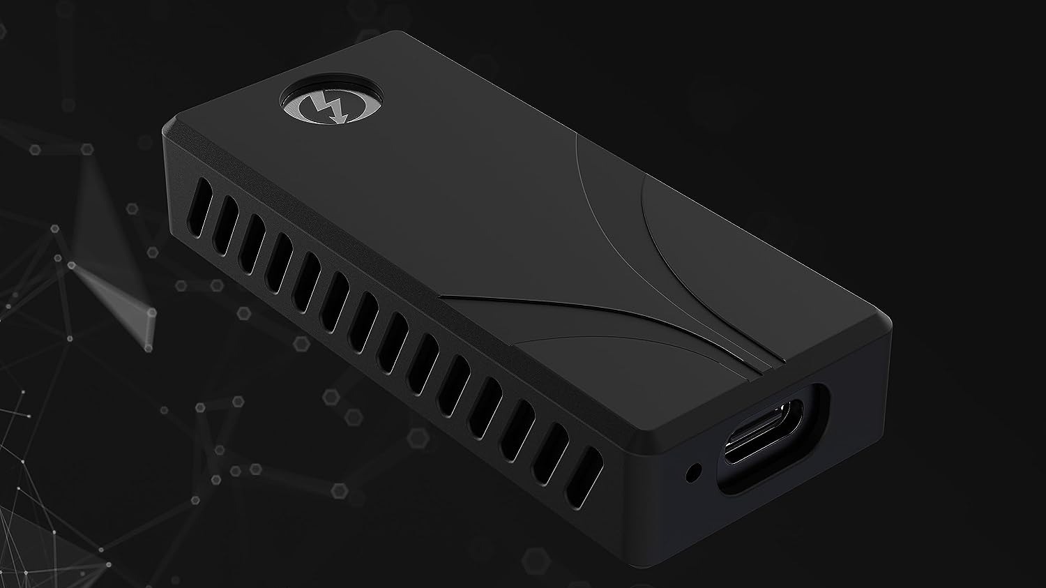
Sabrent has unleashed the company’s new Rocket Nano XTRM (SB-XTMN-1TB) to rival the best external SSDs. Designed to take advantage of Thunderbolt 3, the external SSD offers consumers 1TB of storage with transfer speeds of up to 2,700 MB/s. The Rocket Nano XTRM 1TB retails for $199.99 on Amazon.
The Rocket Nano XTRM measures 2.7 x 1.1 x 0.5 inches and weighs 2.2 ounces. It’s slightly smaller than your typical bank card. The aluminum body helps keep the weight down while providing heat dissipation benefits. The lightweight and compact design lets you take the external SSD anywhere, including inside your shirt pocket. An optional handy silicon sleeve is available to keep the external SSD safe from accidental drops and harsh environments.
The Rocket Nano XTRM uses a USB Type-C connection, allowing it to connect to your desktop PC, laptop, smartphone, tablet, or any other device with a USB-C port. It’s the preferred interface where the Thunderbolt 3-certified external SSD can hit its advertised 2,700 MB/s transfer speeds. The quoted performance shows that the Rocket Nano XTRM is a worthy rival for the SanDisk Pro-G40, which we consider the best portable SSD.
The Rocket Nano XTRM doesn’t necessarily require a USB Type-C port. It is backward compatible with previous USB ports, such as USB 3.2 Gen2x1, but it’ll cripple the transfer speeds to 900 MB/s. Sabrent includes two cables with the Rocket Nano XTRM: a USB Type-C to USB Type-C cable and a USB Type-C to USB Type-A cable. Regarding compatibility, the external SSD works right out of the box on Windows and macOS operating systems without additional drivers or power cables.
The Rocket Nano XTRM 1TB retails for $199.99 on Amazon. However, Sabrent is running a special sale for the external SSD’s introduction, where it can be yours for $169.99 at the company’s store. The Rocket Nano XTRM comes with a one-year warranty. However, registering your product with Sabrent will extend the warranty period to three years.
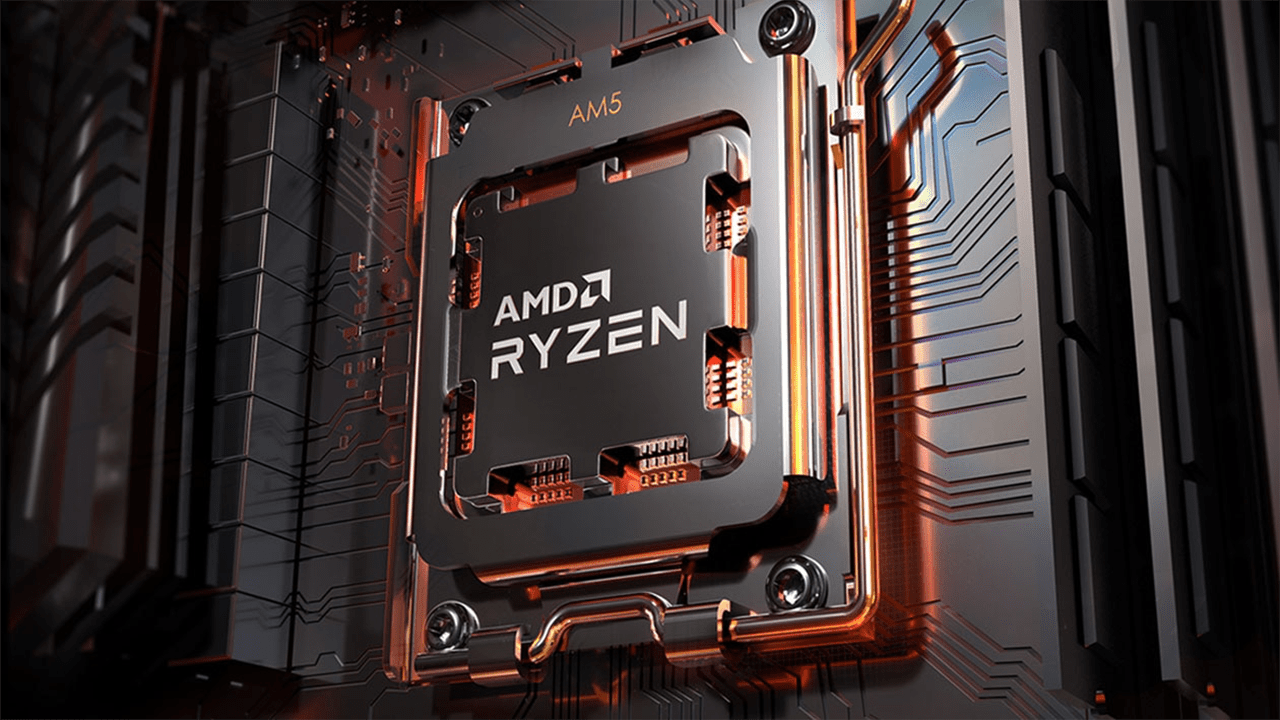
When AMD launched its six-core Ryzen 5 7500F last month, it only released it in retail in China and said that it would be available in other countries to system integrators — and that end-users would only be able to purchase it inside desktop PCs. It seems those limitations didn’t work out, and the cheapest Zen 4-based CPU is now available both in Europe and North America.
ShopBLT, a store known for selling new hardware ahead of others, is now offering the Ryzen 5 7500F for $176.46 or for $181.83 — which is very close to AMD’s recommended MSRP of $179. AMD’s Ryzen 5 7500F processor is designed to bring the benefits of the AM5 platform to budget-conscious gamers anticipating future upgrades, so it is nice to see that it is available at nearly MSRP.
Unfortunately, the CPU is not in stock and is ‘ordered as needed,’ so for now it is only possible to order it and get it within 15 business days. It is likely that over time the processor will be available from other retailers, such as Amazon or Newegg, but for now is only available for pre-order from ShopBLT.
The situation with AMD’s Ryzen 5 7500F availability is slightly better in Europe, where the unit is available from multiple retailers, including MindFactory in Germany for €202 and from Future-X in Austria and Germany for €202, as revealed by Geizhals.eu and VideoCardz.
Swipe to scroll horizontally
Header Cell – Column 0
Street/MSRP
Cores / Threads (P+E)
Base / Boost Clock (GHz)
TDP / PBP / MTP
Ryzen 5 7600X
$249 ($299)
6 / 12
4.7 / 5.3
105W / 142W
Ryzen 5 7600
$229
6 / 12
3.8 / 5.1
65W / 88W
Ryzen 5 7500F
$179
6 / 12
3.7 / 5.0
65W / 88W
For now, AMD’s six-core Ryzen 5 7500F CPU is the cheapest desktop Zen 4-based offering from the company. The processor runs at a base clock of 3.70 GHz and can boost up to 5.0 GHz, which is slightly below the clockspeed of the more expensive Ryzen 5 7600. Detailing further, the Ryzen 5 7500F comes with 6MB of L2 cache, 32MB of L3 cache, supports a dual-channel DDR5 memory system, and has 24 usable PCIe Gen5 lanes. Notably, the ‘F’ in its model number denotes the absence of an integrated GPU, necessitating an external graphics card. However, with a 65W TDP and a locked multiplier, this processor is not easily overclockable.
They say that good things come in threes, and the U.S. is definitely banking on the Lawrence Livermore National Laboratory (LLNL) to deliver just that when it comes to cold fusion. Having achieved their second successful fusion ignition with an energy surplus (meaning that more energy was produced than was required to achieve the fusion reaction itself) within a national lab on July 30th, the U.S. now aims to spur research and facilitate a successful third ignition — and beyond. To do that, the country is ready to invest a further $112M into a dozen supercomputing projects.
Fusion (short for nuclear fusion) refers to the ability to fuse two light atoms into a single, heavier one: a process that when successful, leads to the release of massive amounts of energy in the form of electrons. Unlike fission (which works by breaking down heavy elements such as uranium or plutonium), nuclear fusion is expected to be a safe, nearly-unlimited source of energy. When done right, fusing two light atoms (such as deuterium and tritium, each a hydrogen isotope that carries additional electrons compared to “plain” hydrogen) brings about an energy surplus that is more than four times the amount that fission processes can generate. That also makes it a process worth about four million times the amount of energy released from coal burning (at a per-kilogram basis) — its merits are obvious.
It’s on the back of that promise that the newly-instated Scientific Discovery through Advanced Computing (SciDAC) program combines the two pre-existing programs from the Department of Defense with the aim of streamlining programs invested into solving complex fusion energy problems using supercomputing resources, including exascale systems.
“The modeling and simulation work of these partnerships will offer insight into the multitude of physical processes that plasmas experience under extreme conditions and will also guide the design of fusion pilot plants,” said DoE Associate Director of Science for FES, Jean Paul Allain.
There’s still a lot of work to achieve a sustainable, surplus-energy fuel ignition that actually rockets humanity into a clean, energy-conscious and abundant future, however. The July 30th fusion ignition did provide a higher energy output than was delivered into the light-atom fuel capsule (although it’s unknown how much better it was than the 2.05 megajoules-in, 3.15 megajoules-out achieved in December of last year), but that only takes into account the energy transmitted unto the pellet itself. Unfortunately, the way that energy is delivered into the pellet (via 192 lasers) is still extremely inefficient — LLNL needed to push a staggering 322 megajoules to fire the lasers themselves, which still left the process on a global energy deficit.
But the way forward is to better understand the quantum processes surrounding fusion. Until quantum computers themselves can provide a viable computing platform that can crack that code (and there’s no telling how long that will take — but it’s likely in the decade mark), supercomputers based on standard computing are the best way we have to look into the ordered chaos of processes that occur when the laser strikes the pellet.
The $121M will certainly be a boon there — but it definitely won’t be enough. Yet we humans have this strange way of looking farther ahead — of chasing the carrot — than simply focusing on what is right in front of us. This grant injection is part of that, and a healthy injection into the High performance Computing (HPC) landscape — however small a slice of the total it ultimately turns out to be.
If you’re a Steam Deck owner, you have undoubtedly heard of the Sabrent Rocket 2230, an early retail M.2 2230 NVMe SSD that helped DIYers upgrade once-space-limited Steam Decks. However, even the original Rocket 2230’s 1TB maximum could be tight with modern games and lots of ROMs, but thankfully now you can reach up to 2TB with Sabrent’s follow-up Rocket Q4 2230.
SD cards and external storage can only do so much with the Steam Deck and other handhelds, and if you want easily-portable, high-performance storage, a good NVMe SSD is hard to beat. The Sabrent Rocket Q4 2230 is an easy way to upgrade your Steam Deck, ROG Ally, or other portable device to 2TB of fast internal storage. It doesn’t cut corners by using old technology, it’s relatively fast and efficient, and it’s more than enough to get you gaming on the go. To provide 2TB of capacity in the M.2 2230 form factor while being single-sided, it has to compromise by using QLC flash instead of the faster TLC flash. The QLC flash reduces peak and sustained performance, but the drive performs well enough where it matters.
The drive is supported by a normal retail warranty and comes with Sabrent’s copy of Acronis True Image. The drive arrives with a copper-infused heatspreader label, which might require adjustment in some devices (such as with the EMI sleeve in the Deck). Currently, the only readily available TLC-based option in this form factor is the WD SN740, the client version of the WD Black SN770, although we may see more alternatives thanks to the 232-Layer generation of flash.
The Rocket Q4 2230 is very similar to the Crucial P3 Plus and the Crucial P3. These drives are efficient and generally run cool. Like with the Crucial P3 and P3 Plus, the Rocket Q4 2230 opts for a large pSLC cache, which reduces sustained performance compared to a drive like the Solidigm P41 Plus.
The Micron 2400, another popular 2TB choice for M.2 2230 SSDs, uses the same controller as the P41 Plus — the SMI SM2269XT — but comes with Micron’s QLC flash. That controller tends to be less efficient, and it’s possible the Micron 2400 has a larger pSLC cache, making the Rocket Q4 2230 arguably the best all-around QLC-based option for embedded devices at this time. Let’s see how it performs.
Specifications
Swipe to scroll horizontally
Product
1TB
2TB
Pricing
N/A
$219.95
Form Factor
M.2 2230
M.2 2230
Interface / Protocol
PCIe 4.0 x4 / NVMe 1.4
PCIe 4.0 x4 / NVMe 1.4
Controller
Phison E21T
Phison E21T
DRAM
N/A (HMB)
N/A (HMB)
Memory
Micron 176-Layer QLC
Micron 176-Layer QLC
Sequential Read
N/A
5,000 MB/s
Sequential Write
N/A
3,200 MB/s
Random Read
N/A
480K
Random Write
N/A
750K
Security
N/A
N/A
Endurance (TBW)
N/A
450TB
Part Number
SB-213Q-1TB
SB-213Q-2TB
Warranty
5-Year
5-Year
The Rocket Q4 2230 is currently available only at 2TB for $220 on Amazon. Price swings are common in the SSD market, and the competition’s pricing also varies.
Although Sabrent appears to have left the door open for a 1TB SKU, the 2TB is the only one currently available. It peaks at 5,000 / 3,200 MB/s for sequential reads and writes and 480K / 750K random IOPS. Write speeds can be lower for QLC, although this rated value is below what the drive can achieve, and it has enough speed to saturate the PCIe 3.0 bus present in the Steam Deck.
The drive is warrantied for five years with registration, and the drive can absorb up to 450TB of written data. This endurance rating is more than sufficient for the drive’s use in a device like the Steam Deck. Worries about QLC endurance are not warranted; Micron’s 176-Layer QLC is normally rated for 1,500 program/erase cycles with up to 100,000 in pSLC mode.
Software and Accessories
The Sabrent Rocket Q4 2230 comes with a downloadable, Sabrent-specific version of Acronis True Image which is useful for cloning and imaging. This can be nice to have, especially when working with the ROG Ally. Sabrent also has its own SSD toolbox, which will presumably offer firmware updates for the drive, if applicable.
A Closer Look
Image 1 of 3
(Image credit: Tom’s Hardware)
(Image credit: Tom’s Hardware)
(Image credit: Tom’s Hardware)
The Rocket Q4 2230 arrives in a stylish tin, showing off a mixture of white and copper coloring. While not important, the presentation is attractive and does separate it from many OEM SSDs. The drive’s label operates as a heatspreader as it is made of thermally-conductive copper.
Image 1 of 2
(Image credit: Tom’s Hardware)
(Image credit: Tom’s Hardware)
The Rocket Q4 2230 sports an SSD controller and a single NAND package. The drive is single-sided, which is important for many embedded devices like the Steam Deck — it can be a challenge to pack in 2TB of flash with this limitation.
The Rocket Q4 2230 uses Micron’s 176-Layer QLC (N48R) flash, which is convenient for achieving 2TB in such a small package. In contrast, the original Rocket 2230 was constrained to 1TB because it used Micron’s 176-Layer TLC (B47R).
Using 1Tb dies with TLC flash is possible, as the WD SN740 does with BiCS5, but that flash is less efficient. SK hynix also makes 1Tb dies, but given current stacking technology, we will likely see 232-Layer generation flash tackling this role (aside from maybe BiCS6), such as with Micron’s B58R TLC. This flash is already available on many drives, like the Crucial T700.
The Rocket Q4 2230 is DRAM-less, but the host memory buffer (HMB) feature is supported on Valve’s Steam Deck, ASUS’s ROG Ally, and other devices. This should be sufficient for portable gaming workloads. The drive is also PCIe 4.0, which begs the question: does that make a difference for the Deck? In fact, this drive is somewhat more efficient when restricted to the 3.0 interface, and it’s worth going for new hardware for overall performance and efficiency on a portable platform. Such technology does not often arrive on an older PCIe interface, and with it being backward compatible, there’s little reason not to go with a 4.0 drive.
The Rocket Q4 2230 uses the Phison E21T SSD controller, which we’ve reviewed on multiple products, including the original Rocket 2230 (a.k.a. the Rocket 2230 NVMe 4.0). This controller has a history of providing good performance and power efficiency. The latter is probably more important with battery-powered, portable devices. This controller’s primary competition would include the Silicon Motion SM2269XT on drives like the Micron 2400 and Solidigm P41 Plus, the InnoGrit IG5220, and the Maxio MAP1602. However, the latter two are less commonly found on M.2 2230. The MAP1602, on paper, is faster but can run slower, which offers some flexibility.
Future controllers, like the Phison E27T and Silicon Motion SM2268XT, could usurp its position, although the extra performance doesn’t mean much for the PCIe 3.0 Steam Deck. Efficiency gains would be nice, but these two controllers will still be 12nm. Any gains would more likely come from the flash. One other worthy mention is the Kioxia BG6 with an unknown controller. Kioxia has often used Phison controllers, and the BG6 uses Kioxia’s 162-Layer TLC (BiCS6), giving it some bandwidth uplift. Efficiency remains uncertain.
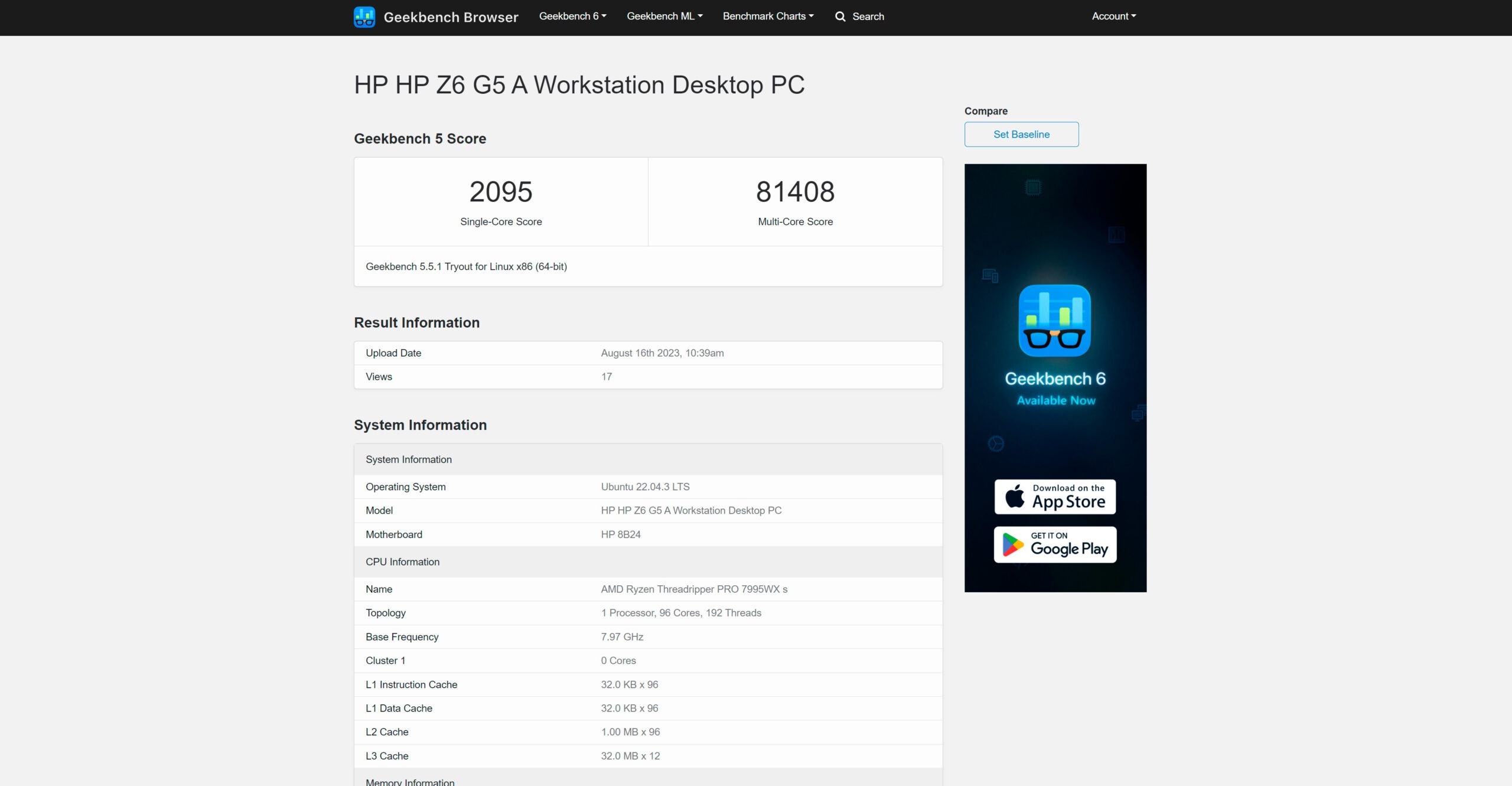
AMD’s forthcoming Ryzen Threadripper Pro 7995WX (Storm Peak) will undoubtedly disrupt the list of best CPUs for workstations. The multi-core beast, which will lead the Ryzen Threadripper Pro 7000WX army, has been spotted in a new benchmark with 96 cores and boost clock speeds up to 5.1 GHz.
The Geekbench 5 submission (via Benchleaks) exposes the Ryzen Threadripper Pro 7995WX with 96 cores and 192 threads. The next-generation workstation flagship represents a 50% increase in core count over the existing Ryzen Threadripper Pro 5995WX (Chagall). It also sports 60% more cores than Intel’s Xeon Platinum 8490H (Sapphire Rapids) server chip.
The Ryzen Threadripper Pro 7995WX is a risky bet on AMD’s part since it’s almost a carbon copy of the company’s EPYC 9654 (Genoa) processor, which retails for $11,805. There will be a difference in features between the Threadripper Pro and EPYC platforms. A handful of processors can compete with Ryzen Threadripper Pro 7995WX regarding core count. Only EPYC Bergamo, which scales up to 128 cores, has more cores.
Ryzen Threadripper Pro 7995WX also comes with a significant upgrade in the cache subsystem. The Zen 4-powered workstation chip wields 384MB of L3 cache and 96MB of L2 cache. That’s the same design on the EPYC 9654. however, in comparison to the Ryzen Threadripper Pro 5995WX, the Ryzen Threadripper Pro 7995WX flaunts 50% more L3 cache and up to 3X as much L2 cache.
Ryzen Threadripper Pro 7995WX Specifications*
Swipe to scroll horizontally
Processor
Cores / Threads
Base / Boost Clock (GHz)
L3 Cache (MB)
L2 Cache (MB)
TDP (W)
Ryzen Threadripper 7995WX
96 / 192
? / 5.1
384
96
350
EPYC 9654
96 / 192
2.4 / 3.7
384
96
320 – 400
Ryzen Threadripper Pro 5995WX
64 / 128
2.7 / 4.5
256
32
280
Xeon Platinum 8490H
60 / 120
1.9 / 3.5
112.5
120
350
*Specifications are unconfirmed.
Ignore the Geekbench 5-reported 7.97 GHz base clock, since it’s an obvious error. However, digging deeper into the Geekbench 5 report shows that the Ryzen Threadripper Pro 7995WX was reportedly boosted to 5,140 MHz, which probably is the single-core boost clock. The Ryzen Threadripper Pro 5995WX has a 4.5 GHz single-boost clock, so the Ryzen Threadripper Pro 7995WX’s rocking a 14% higher single-boost clock.
Compared to the EPYC 9564, the Ryzen Threadripper Pro 7995WX has a 38% higher boost clock. In a way, you could consider the Ryzen Threadripper Pro 7995WX to be a faster-clocked EPYC 9564. An important factor will be the pricing — the EPYC 9564 costs $11,805, so it’ll be interesting to see how AMD prices the nearly-equal Ryzen Threadripper Pro 7995WX.
(Image credit: Primate Labs Inc.)
As with all leaked benchmarks, take these with a grain (or several) of salt. The Ryzen Threadripper Pro 7995WX scored 2,095 and 81,408 points on the single-and multi-core tests, respectively. Compared to the nearly identical Ryzen Threadripper Pro 5995WX submission, the new chip has a 26% higher single-core performance. In terms of multi-core performance, we’re looking at around 49%. The exact numbers will likely differ slightly, so these values are more general ballpark figures.
If the information from a leaked shipping document is legit, the Ryzen Threadripper Pro 7995WX may have a 350W TDP — the same as the Xeon Platinum 8490H. This TDP rating looks reasonable, since the EPYC 9564’s TDP varies between 320W to 400W. In this case, the 96-core Ryzen Threadripper Pro 7995WX seemingly has a 25% higher TDP than the Ryzen Threadripper Pro 5995WX, probably to lodge the extra cores and higher clock speeds.
The leaked document with today’s Ryzen Threadripper Pro 7995WX benchmark hints at an imminent launch for the Ryzen Threadripper Pro 7000WX series. We saw a couple of upcoming Noctua Threadripper CPU air coolers at Computex 2023 with an ETA of October, and the Ryzen Threadripper Pro 7000WX series will likely hit the market around that timeframe.
Foxconn is producing over half of Nvidia-based AI hardware and is benefiting from the brand’s dominance in the artificial intelligence field, according to Economic Daily, citing sources in the supply chain (via TrendForce). Liu Yangwei, the chairman of Foxconn, recently told analysts and investors that the company produces 70% of AI servers sold globally today, reports Commercial Times.
Foxconn appears to be the exclusive maker of Nvidia’s compute GPU modules, such as the A100, A800, H100, and H800. These modules are widely used by all makers of AI GPU-based servers — including Nvidia. The latter offers its customers DGX servers based on A100 and H100 as well as HGX boards powered by the same compute GPUs. And as it turns out, over 50% of HGX boards are also produced by Foxconn.
But Foxcon’s involvement in AI hardware does not end with modules and boards — it also spans to servers and server cabinets, establishing a comprehensive vertical integration that encompasses the whole AI landscape.
Yangwei bragged that the company produces 70% of AI servers, which includes not only Nvidia-based products, but also servers that rely on proprietary AI processors by Amazon Web Services and Google, two large cloud service providers (CSPs). This makes Foxconn one of the largest beneficiaries of the explosive growth of AI servers. (Other beneficiaries include Inventec, Quanta, and Supermicro.)
AI servers is a huge market. Yangwei said that it is projected to expand from $30 billion in 2023 to $150 billion by 2027. To provide perspective on this growth, the entire server market was valued at $123 billion in 2022, and is expected to reach $186 billion by 2027, based on data from IDC.
The head of Foxconn claims that CSPs are the largest consumers of AI servers these days, as they strive to offer their clients appropriate platforms to run various artificial intelligence applications.
He also highlighted that the company’s enduring partnerships with North American CSPs, coupled with its production capabilities in the U.S. — notably the Wisconsin factory — enable it to provide tailored services to major clients like AWS, Google, and Microsoft, granting Foxconn a unique edge in the competitive market.
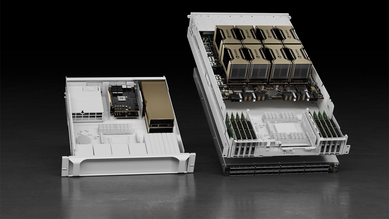
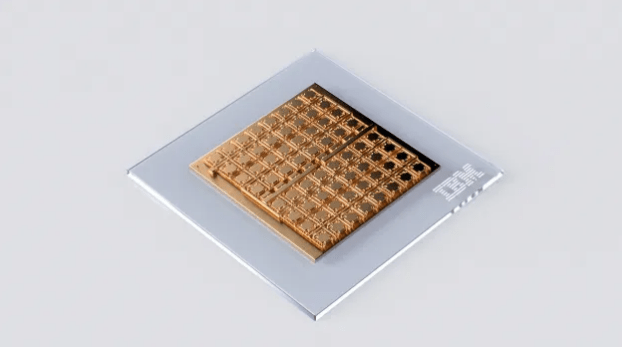
IBM, which has been at the forefront of quantum computing and a number of other research fields, recently showcased what it feels the solution to AI processing (and its costs) could be. And if IBM’s vision translates into something, the future isn’t centered around GPUs: instead, it takes place within mixed-signal, analog chips that could bring about massive improvements in energy efficiency while offering competitive performance against the market’s current go-tos.
According to a research paper published in Nature Electronics last week, IBM believes the future of AI inferencing could pass through a chip combining phase-change memory (PCM) alongside digital circuits. According to the paper, matrix-vector multiplication (one of the main workloads for AI inferencing) could be performed directly on chip-stored weights.
In this scenario, the reduced power requirements of passive, analog circuitry (which don’t require a continuous electrical current to maintain the bit value they’re holding) should allow for a reduction in the overall power required to successfully perform matrix calculations — or, at the very least, allow for the surplus energy budget of the (now) analog sections of the chip to be repurposed towards its remaining digital circuits for added throughput. The design takes clues from learnings from research in neuromorphic computing.
Developed as part of IBM’s Hermes project, the latest version of the chip counts with 64 compute tiles, which communicate with each other through a Network-on-Chip (NOC) approach that’s similar in concept to AMD’s Infinity Fabric. There’s also fixed-function hardware that’s specialized in the processing of convolutional layers (which aim to reduce complexity of the underlying information in order to accelerate processing speed and increase efficiency). Being a research chip, it’s been fabricated at a 14-nm fabrication process; perhaps IBM has room to further improve power efficiency, if the analog cells can be further miniaturized.
The phase-change-memory (PCM) cells themselves are distributed throughout each of the 64 tiles arranged in a crossbar, which can store a 256×256 matrix-vector multiplication space. To be fair, there are certain performance constraints in such a mixed analog-digital design: signals need to be converted from analog to digital (and vice-versa), which incurs penalties in both latency and energy utilization. But with appropriate scheduling optimizations, the final result is higher efficiency compared with a fully-digital chip (such as Nvidia’s A100 and H100). According to IBM, a single ResNet-9 input was processed in 1.52 μs (micro-seconds) and consumed 1.51 μJ (micro-Joules) of energy. According to Abu Sebastian at the IBM Rüschlikon Center (as covered by EE Times), the current iteration of the chip achieves a peak matrix-vector-multiplication throughput of 16.1 to 63.1 TOPC (trillion operations per second) at an energy efficiency of 2.48 to 9.76 TOPS W-1.
The still-ongoing AI “revolution” has sparked volcanic moves in the High Performance Computing (HPC) market. But besides driving home the marvel of GPUs (the general processing units responsible for accelerating most of that particular market), the gold rush for AI accelerators has showcased just how dependent on a single player the market still is (read: Nvidia), while also bringing back to the forefront questions of energy efficiency.
Analog chips that break apart the power efficiency barriers would certainly be a welcome move, but as with any new technology, analog AI inferencing chips will have to fight to survive against the already-entrenched technologies, software stack, and techniques deployed today. Network effects and market share are real, and Nvidia’s grip on the HPC market through both its hardware and CUDA software stacks is… vice-like, to say the least.