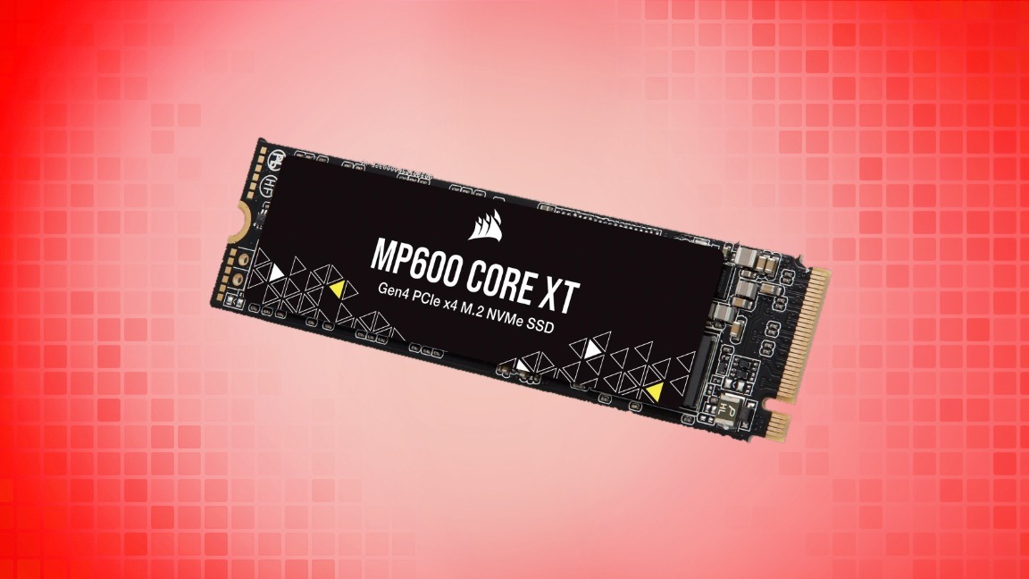
Right now at the official Corsair website, you can find the Corsair MP600 Core XT 4TB SSD for its best price to date. It’s been going for around $199 as of late but is currently marked down to just $159. This SSD isn’t quite industry leading but for a drive in its class, this price is well worh a closer look for anyone looking for more storage at a reasonable price.
We reviewed the Corsair MP600 Core XT SSD earlier this year and regarded its overall performance as mediocre due to its reliance on QLC. However, at this price the offer is much more appealing.
The Corsair MP600 Core XT SSD comes in 1TB an 2TB models but this discount applies only to the 4TB edition. It has an M.2 2280 form factor and connects using a PCIe 4.0 x4 interface. It relies on a Phison E21T controller and uses 176-Layer Micron QLC memory. It can reach read/write speeds as high as 5000/4400 Mbps.
Users can take advantage of optional 256-bit AES encryption for added security. It’s supported by Corsair’s limited 5-year manufacturer’s warranty that voids should the drive reach 900 TBW. Visit the Corsair MP600 Core XT 4TB SSD product page at Corsair for more details and purchase options. As of writing, it’s not clear for how long the offer will be made available.
It’s been a busy year for the best graphics cards, as well as cards that don’t quite make the cut. Not counting third-party cards, we’ve had fourteen “latest generation” consumer GPUs launched over the past year from the three big players. (There are also rumblings of various new GPUs from China, but all indications are that those won’t be competitive with the incumbents any time soon.) As the dust clears, we wanted to take a look back and provide some thoughts on how things have gone down and revisit the recent launches now that we’ve seen the full breadth of the product stacks.
To say that this generation has been a disappointment sums up how most people are feeling. There are some great cards, like the RTX 4090, but it’s priced out of reach of most gamers. Everything below that generally feels overpriced, underperforming, and/or cut specs too far. There are a few exceptions, GPUs that poke above the crowd for one reason or another, but even then there are caveats.
To quickly recap, Nvidia launched the first of its RTX 40-series Ada Lovelace GPUs on October 12, 2022 with the RTX 4090. Then it followed with the RTX 4080 in November, skipped a month and brought out the RTX 4070 Ti (aka the rechristened RTX 4080 12GB) in January, and more recently, the RTX 4070, RTX 4060 Ti, and RTX 4060. Now we’ve completed the set with the RTX 4060 Ti 16GB — slightly late to the party, but it’s done.
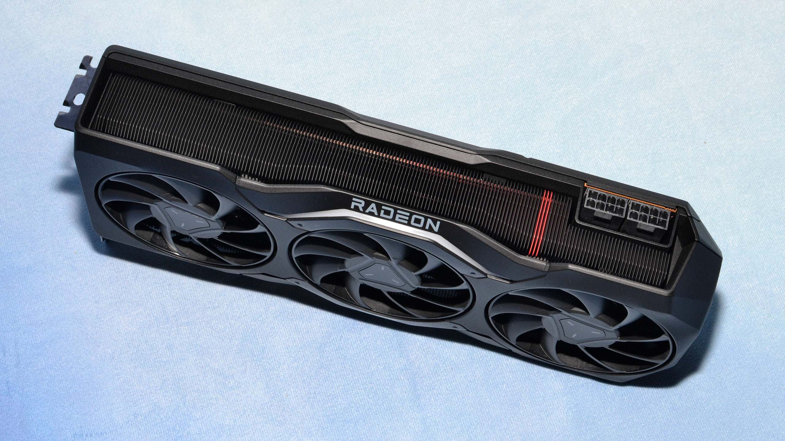
For its part, AMD hasn’t filled in all of the gaps with the new RDNA 3 RX 7000-series GPUs yet, though it’s widely expected that we’ll see the RX 7800-class and RX 7700-class GPUs in the next month or so. (AMD has stated more “enthusiast” GPUs are coming in Q3, which ends in September.) So far, we only have the RX 7900 XTX and RX 7900 XT at the top, and the RX 7600 at the bottom, with the previous generation RX 6000-series holding down the high-end and budget forts.
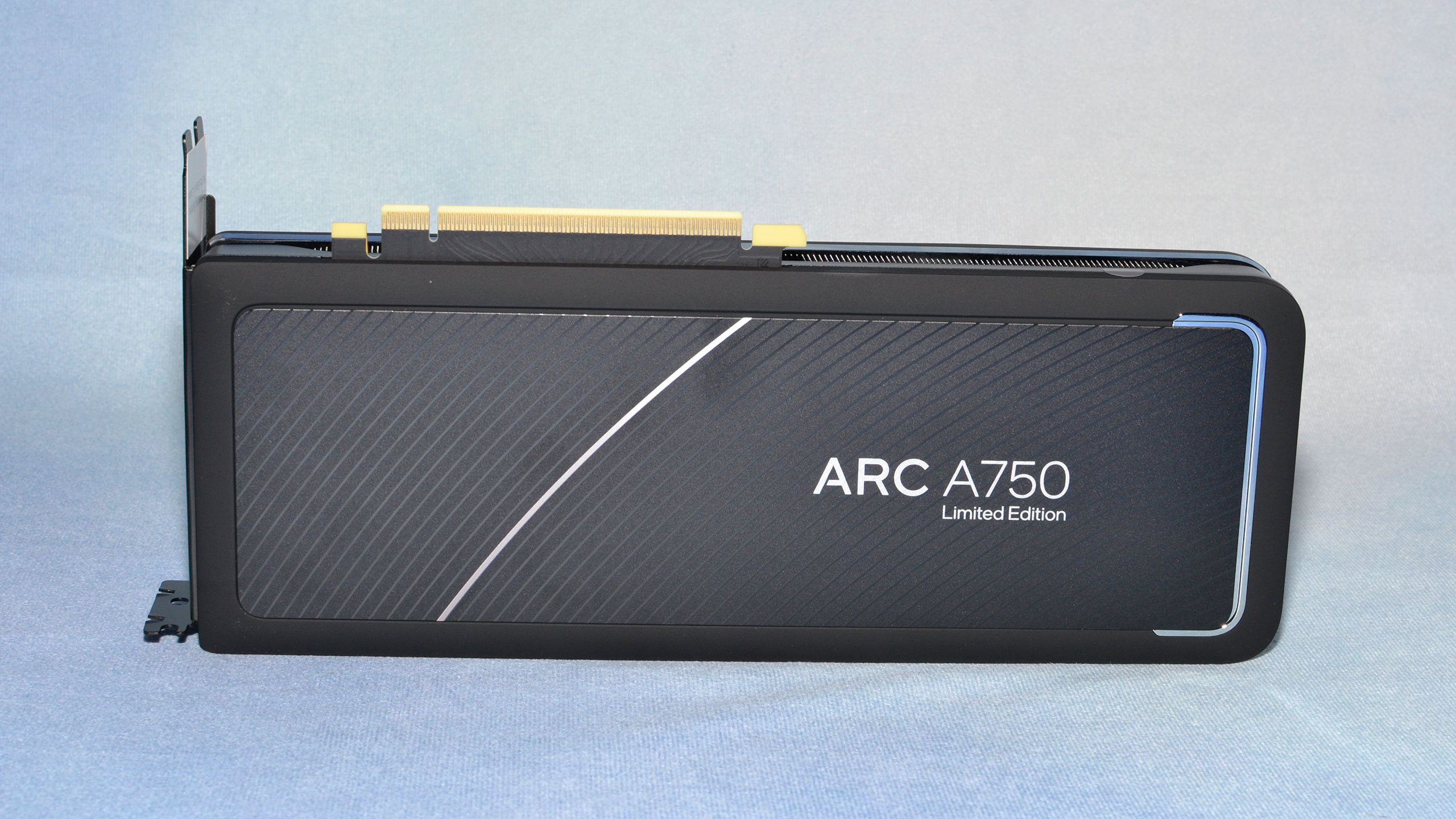
Finally, Intel started shipping its Arc Alchemist GPUs in the U.S. about a year ago, with the Arc A380 blazing trail and clearing out some major driver issues. The Arc A770 and Arc A750 came next, followed by the Arc A770 8GB variant, but the A580 has quietly disappeared. That’s it for the Alchemist generation, but Intel has focused a lot on improving drivers and performance, and we’ll hopefully see the next generation Battlemage sooner rather than later — it has a tentative 2024 launch window, but Intel isn’t commenting on any precise dates yet.
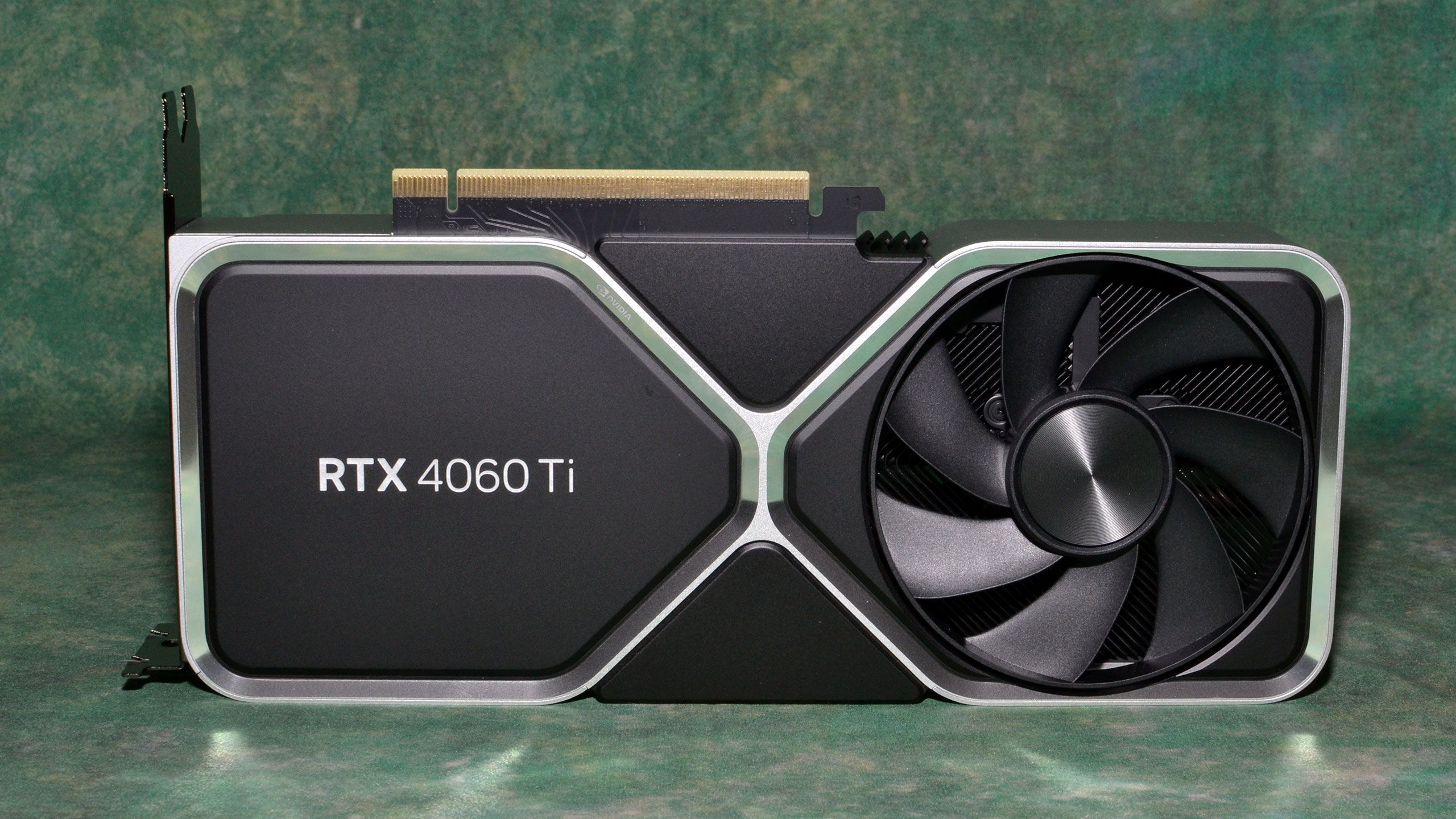
The RTX 4060 Ti, both 8GB and 16GB variants, really showcases how this generation has gone off the rails in certain areas. (Image credit: Tom’s Hardware)
Every GPU launch ends up being a snapshot in time, often one done under an extreme time crunch. Typically, we’ll get briefed on the new GPU about two weeks in advance of the launch, with hardware arriving about ten days ahead of the embargo date. It’s hectic, to say the least. The “top-down” approach to new GPUs also muddies the waters, as we can only compare new products to what is currently available.
The RTX 4060 Ti 16GB launch gives you a good idea of why sampling and embargoes happen. Due to supply (and maybe demand), even though the cards officially launched on July 18, we couldn’t acquire a card at retail until over ten days later. A previously scheduled vacation further delayed things, and our full review was finally posted a month “late.” With no embargo on testing and no hardware sampling, this would become the norm.
But that delayed approach gives us more time to reflect, and with nearly all of the cards now on the table, trends and expectations become much clearer. The latest generation hardware has been pretty weak from a consumer perspective, with only a few exceptions.
We don’t change our scores after reviews go live unless there’s some major mistake. So when we gave the RTX 4090 a 4.5-star score, that’s what we stand by. I actually feel that’s still the right score, but going down through the rest of the product stack, plus looking at GPUs from the competition, my feelings have changed and solidified over time, given the new GPU landscape. So let’s go through each GPU and provide our thoughts about where it currently sits. We also have performance results from our GPU benchmarks hierarchy, plus retail pricing data, which colors our opinions.
Swipe to scroll horizontally
Nvidia RTX 40-Series Ada Lovelace GPUs
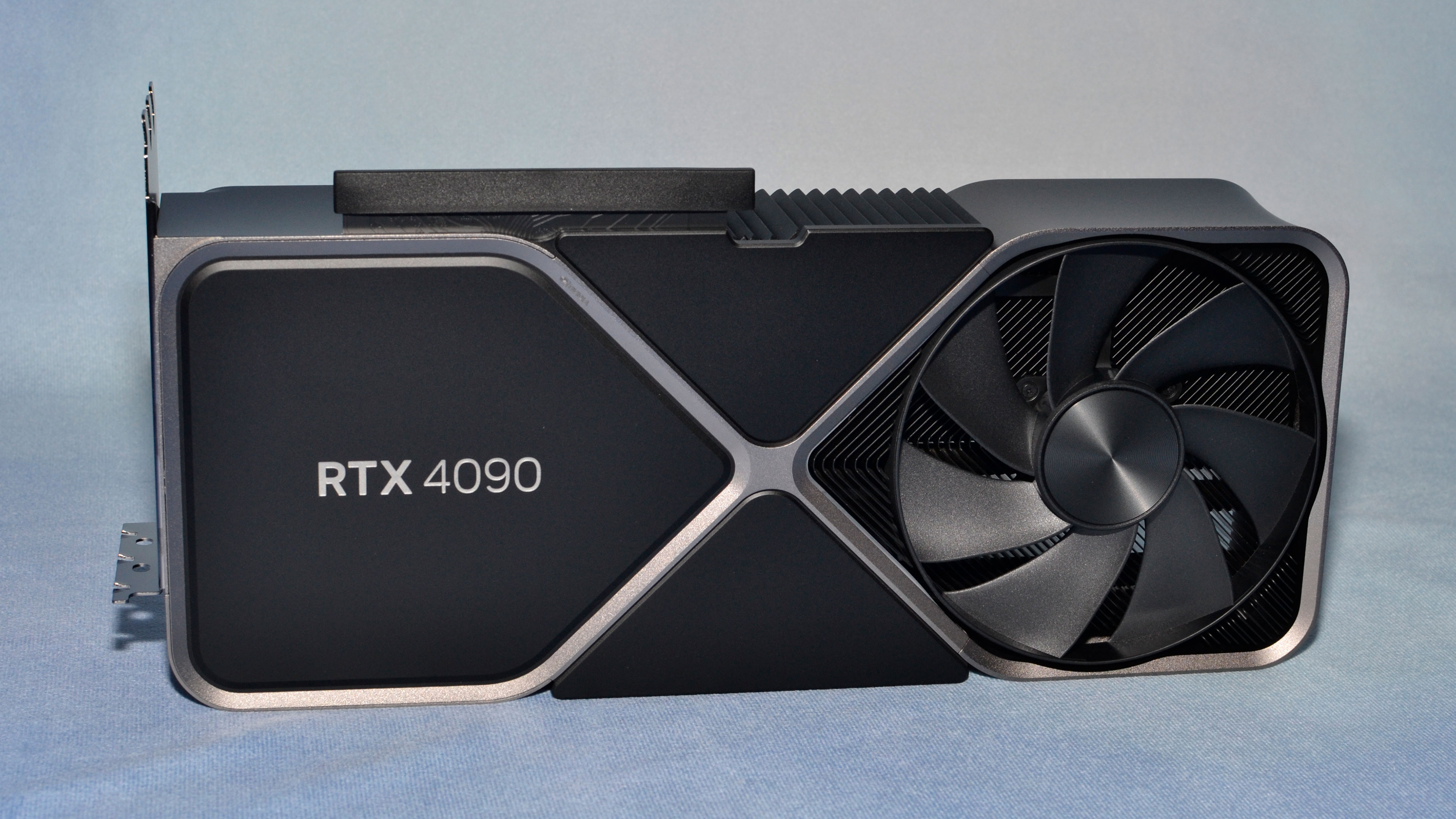
Starting with Nvidia, the RTX 4090 reigns as the fastest graphics card, period. It excels at 4K and starts to hit CPU bottlenecks — even on our Core i9-13900K test PC! — at 1440p and lower. That’s also why its average power draw looks so tame: at 1080p, the GPU ends up waiting on the CPU a lot and doesn’t come anywhere near its 450W TGP (total graphics power) rating, but focusing just on 4K it averaged 394W across our test suite. It’s expensive at $1,599, yes, but if you want the fastest graphics card that doesn’t really compromise anywhere, this is the GPU to get.
Stepping down to the RTX 4080, it’s not nearly as exciting as its bigger sibling. It’s clearly faster than any previous generation GPU, but it costs nearly as much as the 4090 while cutting performance and specs quite a bit. At 4K, for example, the 4090 is 36% faster and costs 33% more — 45% more going by the current lowest-priced retail cards. This felt like a taste of things to come, with lower performance gains and higher pricing compared to the previous generation, and it was. We also would have preferred a 320-bit interface with 20GB of VRAM (double the 3080) rather than 16GB on a 256-bit interface. This now ranks as the second fastest GPU overall, but in our view, it’s still priced about $200 higher than it warrants. It’s simply too high for what you get.
The RTX 4070 Ti echoes the 4080 story: too expensive for relatively minor generation gains in performance — unless you really love DLSS 3 Frame Generation and want to drink the Kool-Aid. DLSS 3 is okay, but the feel of games, when enabled, doesn’t match the supposed performance due to the AI interpolating of frames. It also only has 12GB when we would have liked 16GB, thanks to the 192-bit interface. That’s been a recurring theme in RTX 40-series reviews. Priced $200 higher than the previous gen 3070 Ti, the performance uplift was good (around 50% faster), but the price increase mostly wipes out those gains (e.g. it’s only 20% faster than a 3080 10GB and costs more).
The Nvidia RTX 4090 is still the GPU to beat for this product generation. (Image credit: Tom’s Hardware)
Nvidia’s RTX 4070 at least feels like a move in the right direction. The generational price increase is now “only” $100, though performance is also “only” about 30% faster than the RTX 3070, or on par with the 3080. 12GB on a 192-bit interface also makes this more like a $500-class product, at most, but Nvidia opted to keep prices high. It’s a better value than the 4070 Ti and 4060 Ti 16GB, but that’s not saying much. This was supposed to be the chosen one, as the 970 and 1070 were great cards in their time, but instead of being at the lower end of the high-end price spectrum, it lands in upper high-end territory.
The RTX 4060 Ti 16GB easily ranks as the worst overall prospect for this generation of Nvidia GPUs. Unless you absolutely need VRAM capacity and not bandwidth (or compute), which might help with certain AI workloads, it’s generally not much faster than the 8GB model below. It also takes the price point of the previous generation RTX 3070, and basically matches that card on performance. If this had been the standard 4060 Ti, priced at $399, it would have been far more palatable. Getting a 192-bit interface and 12GB of memory would have sealed the deal. As it stands, we don’t recommend this card.
Cutting the memory in half and going with 8GB, the regular RTX 4060 Ti again feels like Nvidia tried to push a lower tier product into a higher tier naming and price category. Call this an RTX 4060 and price it at the level of the outgoing RTX 3060 and we could accept that. But the 128-bit interface and relatively minor generational performance gains — it’s only 11% faster than the 3060 Ti — leave us wanting a lot more.
Finally, the RTX 4060 might still have some warning signs, like the 128-bit interface and 8GB of memory, but those are far more tolerable at $299 than at $399. Generationally, it’s a 19% improvement over the 3060, and it costs $30 less. We don’t absolutely love it, and it would have looked far better as an RTX 3050 replacement, but outside of the RTX 4090, this is arguably the best latest generation Nvidia GPU, with the 4070 ranking third.
Overall, nearly every RTX 40-series GPU feels like it’s priced $100 to $200 higher than it should have been. That’s likely at least partly a result of all the cryptocurrency mining and pandemic induced GPU shortages of 2021 and 2022. Demand has dropped, supply has improved, and pricing isn’t terrible — even at the current prices, the 40-series GPUs today are all far better purchases than the 30-series was in mid-2021, where an RTX 3080 was typically going for $1,500! But it could have been better. Nvidia isn’t concerned, though, as it’s raking in billions from its AI and data center GPUs now.
AMD RX 7000-Series RDNA 3 GPUs
AMD’s Radeon RX 7900 XTX ranks as the fastest AMD GPU and third fastest overall. (Image credit: Tom’s Hardware)
AMD only has three latest generation GPUs (for desktop) currently shipping, though at least two more are expected to land in the relatively near future. The RX 7900 XTX takes the halo spot, with a fully enabled Navi 31 GPU and the full complement of six MCDs (memory cache dies) providing 24GB of memory. That matches the RTX 4090, though performance on average is still 25% lower. The $999 launch price didn’t feel too egregious, and now cards are selling for $949 (sometimes on sale for as little as $899), and this is still a compelling alternative from Team Red, but it’s not a homerun.
Disabling a few cores and one MCD, the RX 7900 XT felt way too close to the XTX in pricing with its $899 launch price. Things are far better now, with cards starting at around $750. Across our full test suite (which includes a few demanding ray tracing games that heavily favor Nvidia), it goes head to head against the RTX 4070 Ti, but falls behind in the final metric. If you care more about memory capacity (20GB) and rasterization performance, though, this is a great alternative to Nvidia’s GPU at a slightly lower price. We can’t help but note that AMD managed to provide more VRAM in what is ultimately a similarly sized chip (counting MCDs and the GCD) than Nvidia, on the same 5nm-class process node (TSMC 4N is refined N5), all for a lower price.
The RX 7800 XT and RX 7700 (non-XT) are rumored to be coming in September. Based on what we’ve seen from the other RDNA 3 GPUs, we expect only moderately improved performance relative to the existing 6800 XT and 6700 XT. Prices remain an unknown, so we’ll have to wait and see where these land.
The RX 7600 fills in the bottom of AMD’s latest generation GPUs, and we’re not sure there’s room for a lower tier RX 7500 this round. Performance ends up being just slightly better than the previous generation RX 6650 XT, by about 3%. The current price is also higher, around $260 compared to $235, and power use is only slightly better at 150W versus 170W (those are our measurements, not the specifications). It’s basically a lateral move for AMD at the budget-mainstream end of the spectrum and echoes a lot of the trends we saw from Nvidia: not enough bang for the buck.
Intel Arc A-Series Alchemist GPUs
The Intel Arc A750 now rates as the best value among latest generation GPUs (Image credit: Tom’s Hardware)
Wrapping things up with Intel, we had hopes that the Arc A770 16GB would provide some much-needed competition to the GPU space. It arrived late to the party, with driver teething pains, but at least the pricing was reasonable. The 16GB cards haven’t come down too much, still selling at $330 right now, and while we like the large quantity of VRAM, you’d be better off grabbing a discounted RTX 3060 — only slightly less performance, lower power, and the drivers are still better, all for less money. But we’re still rooting for an upset from Battlemage when it arrives next year.
The Arc A770 8GB ended up stuck between the proverbial rock and hard place. Performance is close to the 16GB card, but so is the price — these start at $290 now, just $30 less than the full fat GPU. You still have some driver idiosyncrasies at times, though things have definitely improved, but if you’re staring at the A770 8GB, look down to the next card for a much better pick. It’s only a bit slower but costs a lot less.
Intel’s Arc A750 launched at $289, then got an official price drop to $249, and right now it’s selling for just $199 at Newegg. If you’re interested in giving an Intel Arc GPU a shot, this one’s a no-brainer: The Arc A750 represents the best value among graphics cards, with performance that matches the RTX 3060 and almost catches the RX 6700 10GB, for about $70 less. Yes, power use will be higher, and the drivers still aren’t perfect. But with over 30 driver releases since Arc first appeared, the Arc experience today is much better than last year.
Last and perhaps least, we have the Arc A380. It was the scouting party for Arc, and it was poorly equipped when it got shoved out the door. The drivers were frequently broken, and the China-first launch to try and avoid negative publicity didn’t help. Even with all the driver updates, performance remains somewhat questionable. But it’s very inexpensive at just $100, and if you don’t have high graphics requirements, it’s worth a thought. The video encoding support is also good, if you’re interested in that sort of thing.
Closing Thoughts
With fourteen GPUs launched, and probably at least two more to come — maybe even five if AMD does something below the RX 7600 and Nvidia dares to try making an RTX 4050 — plus all of the previous generation cards that are still readily available at often reasonable prices (at least for the RX 6000-series and a few lower tier RTX 30-series cards), there are a lot of choices for anyone looking to pick up a new graphics card. But most people gravitate toward the latest and “greatest” offerings, assuming they’ll be better than what came before, so we’ve provided our thoughts on every current-generation card.
The GPU industry traditionally catered to gamers, but now supercomputing and AI are taking a lot of the demand and production at the high end. Cryptocurrency mining has died off, for the most part, but the effects of the last surge are still being felt. The result is that prices increased in most cases for the same level of hardware, sometimes without the expected bump in performance. It’s been a generally disappointing cycle.
Outside of the top RTX 4090 and bottom RTX 4060 (for now?), Nvidia’s latest cards haven’t really won any friends among gamers. Sure, they’re faster than the previous generation, but they also cost more. AMD hasn’t really done any better, and Intel doesn’t have a previous generation with which to compete — unless you want to somehow count integrated graphics. It was a similar situation back in 2018 with the RTX 20-series that often underwhelmed relative to their predecessors, but the 30-series attempted to correct that. And it would have succeeded if it hadn’t been for those pesky crypto-kids!
Hopefully, history will repeat that pattern, and the next generation RTX 50-series, RX 8000-series, and Arc B-series parts will deliver much more compelling price and performance. For now, with over a dozen new GPUs arriving in the past year, few have managed to rise above the rest. Most aren’t awful, but neither are they amazing. They’re mostly milling around in the middle ground of mediocrity while we wait for more parts that are clearly better than average.
If you can’t wait any longer, in our view, the best current options consist of the RTX 4090, RX 7900 XT, RTX 4070, RTX 4060, and Arc A750. Other new cards might scratch your particular itch, so that’s by no means an exclusive list, but we’re getting close to the half-way point for this cycle. If you haven’t purchased a new GPU within the next few months, you’re probably just as well off sitting back and waiting to see how the next generation fares.
Baikal Electronics, a Russian developer of processors and system-on-chips, is gearing up to develop AI processors to address the country’s needs for artificial intelligence applications. The venture expected to span three years and costing potentially 2 billion rubles ($21.25 million), according to estimates by a former employee of MCST, another Russian CPU developer.
“A new division has been formed to develop a lineup of specialized chips for artificial intelligence, which will adopt the best architectural practices existing at the moment,” said Andrey Evdokimov, chief executive of Baikal, in an interview with CNews. “A key task for the team is to build a software ecosystem for the new processors.”
The new division will focus exclusively on building application-specific integrated circuits (ASICs) for artificial intelligence application. The high-ranking executive of the company did not mention whether its ASIC will be designed for training or inference, or will be optimized to run both type of workloads, like Nvidia’s high-end GPUs. In fact,specific aspects like the project timeline, financial commitments, and intricate details of the chip development remain confidential.
When it comes to hardware used for AI training and inference, Nvidia leads the market and effectively monopolizes certain segments of AI hardware solutions. Meanwhile, export of high-end Nvidia products, such as A100 and H100, to China and Russia is barred by the U.S. export rules.
“The leader in the development of specialized chips for artificial intelligence is Nvidia, which can effectively be considered a monopolist in certain segments of hardware solutions,” said Maxim Maslov, the lead developer of AI ASICs at Baikal. “The export of Nvidia products to Russia is officially prohibited, and there are also restrictions on exporting advanced solutions to China.”
While Nvidia has developed cut-down A800 and H800 versions of its compute GPUs for China, it does not look like these parts are available for Russian customers.
“Despite the critical importance of specialized hardware for the development of artificial intelligence technologies, the gap between leading global and Russian developments is evident,” Maslov added. “Existing domestic solutions are niche and do not cover the entire spectrum of necessary tasks, lacking the necessary software ecosystem.”
Baikal believes that this gives the company a chance to address Russia’s needs for AI hardware in the coming years. What is unclear is where Baikal plans to produce its AI chips. Taiwan restricts shipments of advanced processors to Russia and Belarus, so TSMC and UMC can be excluded from the list of potential makers. U.S.-based Intel and GlobalFoundries are also unlikely candidates due to sanctions against Russia by the U.S. and Europe. In theory, China-based SMIC can make certain chips for Baikal, but it may turn such orders down fearing further scrutiny from the U.S. government.
Amazon Web Services and Google also have their own AI processors for training and inference and they are available in the cloud. Meanwhile, it is unclear whether Russian companies use these AI cloud services.
When it comes to creative solutions, no one’s better up to the task than maker and developer Ivan Kuleshov. Whether he’s hacking a Mac Mini to use PoE or developing the new soon-to-be-released Compute Blade module, Kuleshov’s creative juice is in no short supply. Today we’re sharing another project of his shared to Twitter/X, this time a medley of both Raspberry Pi and Mac Minis. Kuleshov ran into an issue recently in which a rack of 16 Mac Minis needed to be manually powered on. His solution? Use a Pi to flip the physical switches, of course!
The Pi is connected to 8 individual servo motors that are responsible for activating the power switch on two Mac Minis a piece. The Raspberry Pi is fitted with a PiKVM HAT so it does more than just power on the Mac Minis. This also meant that developing a custom case was necessary to support the additional hardware.
This project is more than just a proof of concept. We spoke with Kuleshov who confirmed the setup has successfully been implemented in a professional setting. His team works in a data center that has three shelves of Mac Minis and this Raspberry Pi rig is able to power them on using the system of servos.
Image 1 of 3
(Image credit: Ivan Kuleshov)
(Image credit: Ivan Kuleshov)
(Image credit: Ivan Kuleshov)
The Raspberry Pi has a couple of HATs and extra hardware that required Kuleshov’s cool case design. It fits the Raspberry Pi, a PiKVM HAT, a Servo HAT and an OLED screen. A heatsink and fan were included to cool the unit, as well. The outer housing is also fitted with LEGO-compatible studs so you can attach your favorite LEGO pieces—his team chose a Stormtrooper figure.
The software involves a custom UI that Kuleshov put together that makes it easier to operate the PiKVM features and servos. Python was used to program the servos while some bash scripts enable it to interact with a separate KVM switch.
To get a closer look at this Raspberry Pi project, check out the original post shared by Ivan Kuleshov. You can also follow him at Twitter/X or Instagram to keep an eye out for future creations as well as any updates on this one.
Google has cancelled its codenamed Agah, Hades, and Herobrine Chromebooks motherboards reference designs with discrete GPUs, which signals that the company may have cancelled its higher-end gaming Chromebooks project in general, reports Ars Technica. Of course, it is possible that the company cancelled these parts to focus on something else, but it does not look like Chromebooks with standalone GPUs are around the corner.
“Herobrine, Hades, and Agah are all cancelled,” a developer wrote in a comment for an AboutChrombeeks post. “The infra (overlays, builders, etc.) have already been shut down for them. Delete.”
Google initiated a project to design gaming-centric Chromebooks back in 2021 in a bid to grab another part of the enthusiast PC market. Although these devices boasted things like customizable keyboards with RGB lighting effects and displays with high refresh rates, their reliance on integrated GPUs predestined their usage primarily for cloud gaming platforms, like Nvidia’s GeForce Now and Microsoft’s Xbox Cloud Gaming.
Excitement grew late in late 2022 when signs of a more locally gaming-oriented Chromebook emerged. Reference motherboard codenamed Hades came with a discrete GeForce RTX 4050 GPU, a chip that is set to power entry-level Windows-based gaming laptops. In addition, Google developed Agah and Herobrine reference designs with standalone Nvidia graphics processors. As a result, Chromebooks based on these boards will not make it to the market. Unless, of course, some prominent Chromebook backers decide to proceed with a Chromebook featuring a discrete GPU themselves.
There undeniably existed a potential market for these gaming Chromebooks. With their widespread use in educational settings, students could have benefited from a game-capable Chromebook running a familiar platform. However, the project would have inherited common gaming laptop peculiarities, such as higher power consumption and shorter battery life, which is crucial for students.
But gaming on ChromeOS is riddled with obstacles. Google had managed to adapt the Linux-based Steam client for Chrome OS. With ChromeOS’s inherent Linux architecture, it can run numerous Windows games through the Proton layer. Yet, there were hurdles. As of November 2022, crucial software like anti-cheat systems for several online games remained incompatible. Other issues, such as performance lags on 2560×1440 and 4K displays and the necessity for storage workarounds for certain game installations, plagued the system.
In fact, the complexities of porting Windows games to Linux and Linux applications to ChromeOS would have made these machines considerably less appealing than traditional Windows laptops for gamers. This, combined with an overall dip in the PC market and the intricacies of integrating Nvidia GPU drivers into ChromeOS, may have influenced Google’s decision to abandon the endeavor.
OLED displays are becoming more commonplace in the world of laptops. They promise richer and more saturated color and deliver inky blacks unmatched by other panel types offered on laptops. So, color me surprised when the Acer Swift Edge 16 made its way into the Tom’s Hardware lab, complete with a 16-inch OLED display with a price tag of less than $1,300.
However, it’s not just the display and price that impress; the Swift Edge 16 comes with a potent Ryzen 7 7840U processor, a comfortable keyboard with a number pad, the rare inclusion of a 1440p webcam along with a thin and lightweight chassis that makes it an easy travel companion when compared to the best ultrabooks and premium laptops.
Acer Swift Edge 16 Specifications
Swipe to scroll horizontally
CPU
AMD Ryzen 7 7840U
Graphics
AMD Radeon 780M Graphics (Integrated)
RAM
16GB LPDDR5-6400 (non-upgradeable)
Storage
1TB NVMe PCIe 4.0 x4 M.2 SSD
Display
16-inch, OLED, 3200 x 2000, 120Hz
Networking
Wi-Fi 6E, Bluetooth 5.1
Ports
2x USB 4 Type-C, 2x USB 3.2 Gen 1 Type-A, 1x HDMI 2.1, 1x 3.5 mm jack, 1x micro SDXC slot
Camera
1440p
Battery
54 WHr
Power Adapter
65W
Operating System
Windows 11 Home
Dimensions (WxDxH)
14.08 x 9.68 x 0.60 inches (357.5 x 245.9 x 15.24 mm)
Weight
2.73 pounds (1.24 kg)
Price (as Configured)
$1,299.99
Design of the Acer Swift Edge 16
“Sleek” and “thin” are the first two words that sprung to mind when I first took the Swift Edge 16 out of the box. The laptop is just 0.6 inches thick with the lid closed, allowing it to slip into a bag easily. That thinness is accompanied by a total weight of 2.73 pounds, which is roughly half a pound lighter than the 15-inch Apple MacBook Air.
However, that difference in weight between the two machines is exacerbated by the materials chosen by Apple and Acer, respectively. The former goes with an aluminum unibody that exudes quality and sturdiness. However, the latter uses a cheap, thin plastic upper chassis and an equally thin aluminum lower chassis cover. As a result, the chassis easily flexes and doesn’t elicit confidence in long-term durability.
Image 1 of 6
(Image credit: Tom’s Hardware)
(Image credit: Tom’s Hardware)
(Image credit: Tom’s Hardware)
(Image credit: Tom’s Hardware)
(Image credit: Tom’s Hardware)
(Image credit: Tom’s Hardware)
I lightly pressed on the palm rest directly to the right of the touchpad and watched as the entire keyboard deck dipped down at least an eighth of an inch in response. The sub-3-pound weight is admirable, but it’s immediately apparent what sacrifices were made to achieve this figure.
The right side of the chassis is home to a USB 3.2 Gen 1 Type-A port, headphone jack and a microSD card slot. The opposite side gives you an additional USB 3.2 Gen 1 Type-A port, two USB4 Type-C ports and an HDMI 2.1 port. The Swift Edge 16 charges via one of the two USB-C ports using a 65-watt power adapter. Unlike competing USB-C chargers from Apple and Samsung, Acer’s power brick and USB-C cord are attached instead of being two separate pieces.
A full-size keyboard sits front and center, with a narrow number pad off to the side. A 3.4 x 5.1-inch touchpad sits off-center below the keyboard.
However, the star of the show is undoubtedly the 16-inch OLED display, surrounded by relatively thin bezels all around. This is a 120 Hz unit that is VESA DisplayHDR True Black 500 certified. Like many OLED panels, this one features a glossy coating, which is meant to improve the clarity of the picture. While that may be the case, the glossy finish was a magnet for reflections in my home office. Sitting above the display was another surprise, a 1440p webcam.
The Swift Edge 16 measures 14.08 x 9.68 x 0.60 inches, giving it a slightly larger footprint than the 15-inch MacBook Air. It’s also marginally larger dimensionally than the Lenovo Yoga 9i, a 3.09-pound, 14-inch convertible. The 15-inch Microsoft Surface Laptop 5 measures 13.4 x 9.6 x 0.58 inches and weighs 3.4 pounds.
Acer Swift Edge 16 Productivity Performance
The Swift Edge 16 uses an AMD Ryzen 7 7840U, an octa-core processor with a 3.3 GHz base clock and a 5.1GHz turbo clock. Acer configures the laptop with 16GB of LPDDR5 memory and a 1TB SSD.
Image 1 of 3
(Image credit: Tom’s Hardware)
(Image credit: Tom’s Hardware)
(Image credit: Tom’s Hardware)
Starting with the Geekbench synthetic CPU benchmark, the Swift Edge 16 virtually tied with the MacBook Air (M2, 16GB RAM) in the single-core benchmark (1,899). However, in the multi-core test (9,624), the Swift Edge 16 bested the MacBook Air and came in second to the Yoga 9i (Core i7-1360P, 16GB RAM), which scored 9,954.
In our file transfer test, which copies 25GB of files, the Swift Edge 16 hit 1,269.79 MBps. That was good enough for third place behind the MacBook Air (1,342.38 MBps) and the Yoga 9i (1,669.29 MBps). The Surface Laptop 5 (Core i7-1265U, 16GB RAM) wasn’t a contender, delivering just 532.52 MBps during the test.
The Swift Edge 16 took an easy win in our Handbrake test, which involves encoding a 4K video to 1080p. The laptop completed the task in just 7 minutes and 18 seconds, putting it 28 seconds ahead of the MacBook Air. The Yoga 9i was the laggard in this group, requiring 9:45 to finish.
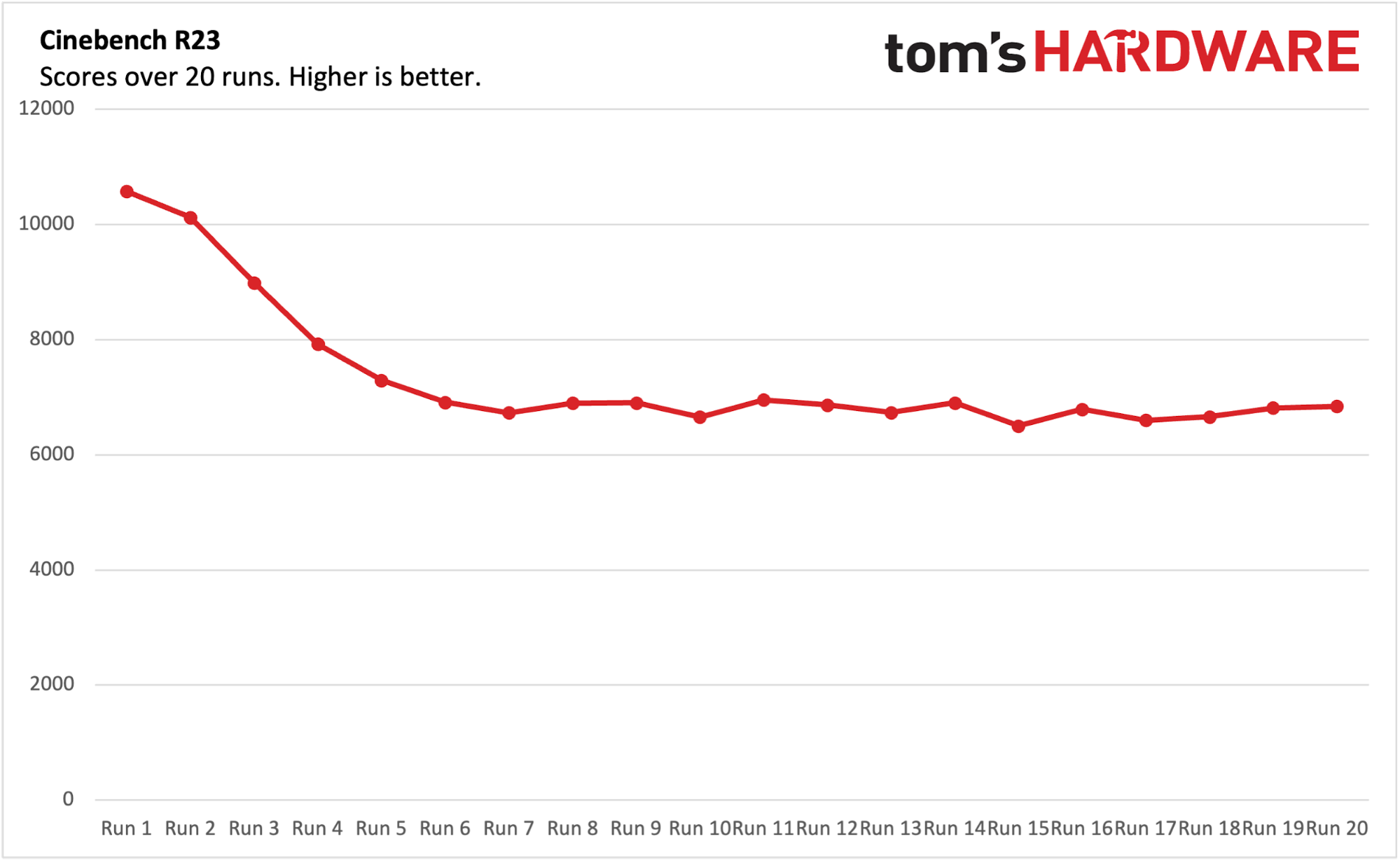
(Image credit: Tom’s Hardware)
In our Cinebench R23 stress test, we perform 20 runs and record the scores. The Swift Edge 16 started the test with a score of 10,575.95, declining significantly from there as heat ramped up. Scores leveled off in the 6,600 to 6,800 range after about seven runs. During the test, the Ryzen 7 7840U chugged along at 2.04GHz and 58.91 degrees Celsius (138.03 degrees Fahrenheit).
Display on the Acer Swift Edge 16
The Swift Edge 16 features an OLED display, which is a welcome inclusion in the sub-$1,500 price category. As the laptop’s name implies, the panel measures 16 inches across and has a 3,000 x 2,000 resolution (3:2 aspect ratio, which we’re used to seeing in Microsoft’s Surface family) and a 120Hz refresh rate. Acer claims that the panel is VESA DisplayHDR True Black 500 certified.
I found the display to be bright enough for typical use, but the glossy coating couldn’t shake the reflections I saw. Not only could I see my reflection staring back at me (particularly apparent with dark content) in my home office, but the effect was only exacerbated outside in the sunlight.
(Image credit: Tom’s Hardware)
With that said, when the lighting was ideal, the rich colors and inky blacks of the OLED panel were a joy to behold. Although I went to see The Super Mario Bros. Movie in the theater, its recent digital release meant that I had to purchase the movie for my kids to watch over (and over, and over again). This was the perfect movie to showcase the Swift Edge 16’s display, with its rich color palette (particularly when Mario visits the Mushroom Kingdom). Likewise, Luigi’s descent into the bowels of the Dark Lands highlighted the excellent contrast.
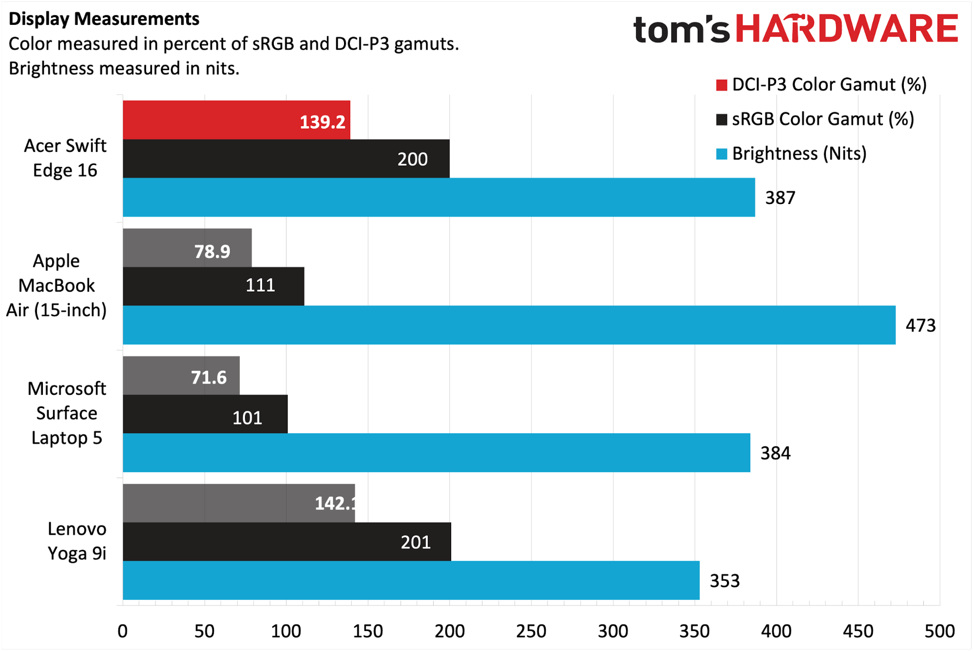
Our instrumented testing confirmed what my eyeballs were seeing, with the Swift Edge 16 hitting 139.2 percent of DCI-P3 and 200 percent of sRGB (closely matching the performance of the OLED in the Yoga 9i). Brightness was also second only to the MacBook Air, coming in at 387 nits.
Keyboard and Touchpad on the Acer Swift Edge 16
The keyboard on the Swift Edge 16 felt good under my fingers, providing comfortable feedback with quiet operation. The feel of the keys reminds me of a close approximation to that of current-generation MacBook keyboards. Given the productivity-centric purpose of the laptop, there are no RGBs found here, although there is a soft white light that glows beneath the keys (and turns off after about 30 seconds to save power).
(Image credit: Tom’s Hardware)
A narrow number pad, which is an increasingly common feature for 15- and 16-inch class laptops, is available for quick number entries. I appreciate its inclusion for making quick calculations and entering data into spreadsheets.
My go-to for typing tests is keyhero.com, and I managed to type at 85.03 words per minute with 97.91 percent accuracy. For comparison, I averaged 75 wpm and 90.61 percent accuracy on the similarly-sized Samsung Galaxy Book 3 Ultra using the same test, so I much preferred this keyboard.
Audio on the Acer Swift Edge 16
The Swift Edge 16 has two speakers, backed by Acer TrueHarmony technology. Acer claims that TrueHarmony provides more powerful, “headphone-like audio,” but that wasn’t my experience.
The audio was as lifeless as you’d expect with a laptop this thin and light. The speakers weren’t overly loud even with the volume cranked to 100 percent. With that said, they were distortion-free at this volume. I dialed the volume back to about 60 percent and played Guns N’ Roses’ “November Rain.” No matter the volume level, the audio sounded thin and hollow from the downward-firing speakers. OK, maybe it’s a tall order to expect perfection when reproducing audio from one of the greatest rock songs of the 1990s on a $1,300 laptop, especially one that is so svelte, but non-existent bass and no attention to the highs leaves much to be desired.
If you want to use the Swift Edge 16 to handle video calls or watch YouTube videos while doing other tasks, the speakers will suit you just fine. However, grab a pair of good headphones if you want to actually enjoy music.
Upgradeability of the Acer Swift Edge 16
The Swift Edge 16’s internals are accessible by removing six T6 screws on the bottom of the chassis. With the screws removed, I stuck my thumbnail near one of the USB ports and carefully pried off the panel.
Unfortunately, there’s not much to see once inside; the battery is replaceable, as is the M.2 SSD (although there is only one M.2 slot for storage). The Wi-Fi 6E/Bluetooth combo card is also replaceable if you so choose. The LPDDR5 memory is soldered onto the motherboard, so there are no provisions for upgrading your memory from the standard 16GB in the future. This is, unfortunately, increasingly common on thin PCs.
Battery Life on the Acer Swift Edge 16
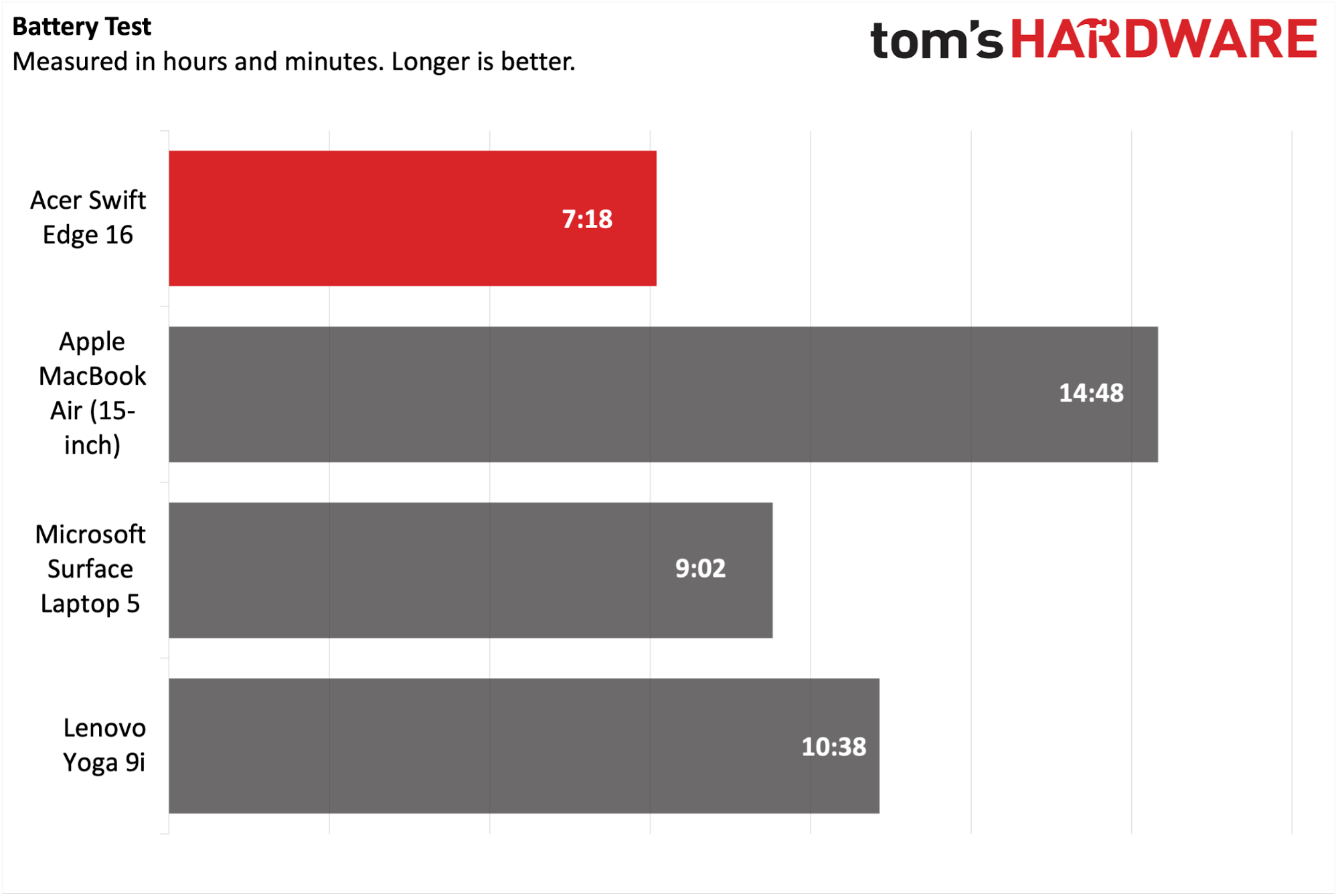
Among its competitors the Swift Edge 16 wasn’t a standout in our endurance test (web browsing, light graphics work and video streaming while connected to Wi-Fi with Swift Edge 16’s display brightness set to 150 nits). It finished at the back of the pack (7:18).
(Image credit: Tom’s Hardware)
The Surface Laptop 15 lasted nearly two hours longer, while the Yoga 7i gave up after 10 hours and 32 minutes. However, the MacBook Air was the endurance champion, lasting almost 15 hours on a charge.
Heat on the Acer Swift Edge 16
We take the skin temperature of ultrabooks while running the Cinebench R23 stress test to see how they deal with heat. During the test, the Swift Edge 16’s fans spun up noticeably to exhaust heat generated by the Ryzen 7 7840U. The aluminum bottom panel of the chassis was warm to the touch but was not uncomfortable to rest on my lap.
I measured 39.9 degrees Celsius (103.83 degrees Fahrenheit) between the G and H keys, while the touchpad was much cooler at 29.4 C (89.42 F). The bottom of the laptop saw the hottest temperatures, reaching 51.5 C (124.7 F) towards the left-rear corner.
Webcam on the Acer Swift Edge 16
With most new laptops coming out with 1080p webcams, it’s becoming harder to notice any significant differences between them. However, Acer is trying to one-up the competition with a 1440p webcam on the Swift Edge 16.
I didn’t expect a dramatic difference in quality compared to the 1080p competition, and my results confirmed that hypothesis. However, the details were incredibly crisp, the colors looked spot-on, and image noise was practically non-existent.
Acer doesn’t offer a physical privacy shutter for the webcam or a hotkey to deactivate it quickly. The webcam also isn’t Windows Hello compatible. You also won’t find other biometric security features like a fingerprint reader.
Software and Warranty on the Acer Swift Edge 16
Acer goes easy on the installed apps, as there isn’t much bloatware here. There’s an Acer product registration app, and the handy Acer Purified Voice Console allows you to configure microphone settings. Acer Care Settings monitors your system vitals (SSD, memory, battery health), performs system updates and can backup/restore your system – it’s a nice one-stop-shop for configuring the laptop. The only other preinstalled app from the factory is the venerable Realtek Audio Console.
Of course, you can expect to find the usual app shortcuts placed by default with each Windows 11 Home install, like Kindle, WhatsApp, and Spotify.
Acer provides a one-year manufacturer warranty with the Swift Edge 16.
Acer Swift Edge 16 Configurations
Our review unit features an AMD Ryzen 7 7840U processor, 16GB of RAM, a 1TB PCIe 4.0 SSD, and a 16-inch 3,200 x 2,000 OLED display. This model is exclusive to Best Buy and priced at $1,299. However, this configuration frequently goes on sale and was recently available at Best Buy for as low as $1,099. There’s also an older SKU with a 3840 x 2400 OLED display, Ryzen 7 7735U processor and a fingerprint reader for $1,299 (although it is often on sale at Costco for $899).
Bottom Line
The Acer Swift Edge 16 has a lot going for it. It’s lightweight and thin for this class, the 16-inch screen is gorgeous, and performance was strong across the board. Even better, the $1,299 price tag ($1,099 if you can grab it on sale) is quite compelling for a large-screen OLED laptop.
On the other hand, the speakers are subpar, the quality of the materials used (particularly the keyboard deck) could be better and battery life ranked at the bottom of the pack. The first issue is easily solved with a pair of headphones, while the second doesn’t feel as premium — or as durable — as other laptops in its class. As for endurance, seven hours of battery life is disappointing, especially compared to the 10-hour showing of the Lenovo Yoga 9i and the nearly 15-hour runtime of the 15-inch Apple MacBook Air.
The Yoga 9i is a fine alternative (if you like the convertible form factor and don’t mind the 14-inch display) due to its similar performance, sturdier construction, and longer battery life. The laptop also regularly goes on sale for $1,149, making it an even more compelling choice. The Swift Edge 16 still has a lot to offer, but perhaps a future update can address our battery life and durability concerns.
Even with proper bed leveling and one of the best 3D printers, sometimes you can experience issues with your 3D prints not sticking well to the 3D printer bed either because of the nature of the design you are printing or the type of material you are using. One of the ways to address this issue is by using a brim.
A brim is an additional thin material you add to your design in the slicer to improve adhesion between the printed object and the 3D printer bed. It achieves this by increasing the contact area between the object and the build plate, providing better stability and preventing warping or detachment during printing. A brim is not intended to be a permanent part of the final 3D printed object. Once you finish 3D printing, you can remove it.
Benefits of 3D Printing Brim
Some of the benefits of a brim in your designs include:
Improved adhesion: As we have mentioned above, the primary purpose of a brim is to enhance adhesion between the print and the build platform, reducing the likelihood of issues resulting from poor adhesion. Also, you will not need adhesion aids like glue sticks or hairspray to help the print attach to the bed.
Stability: For objects with complex geometries and overhangs, adding the brim will act as an anchor, preventing those parts from detaching or becoming misaligned.
Minimized warping: A brim helps counteract the effects of differential cooling, which can cause warping in materials like ABS. The extended surface area improves bonding, reducing the risk of warping.
Adaptability to print speeds: A brim is particularly valuable when printing at higher speeds, as it helps counteract the increased forces that can make the print more prone to lifting or shifting.
Cleaning up the design is easier:Post-processing your 3D prints, especially on the bottom section, is easier as you can peel away or trim the brim easily without affecting the design itself. Also, you can easily clean any remaining traces on the object without affecting the part itself, unlike when it was 3D printed without it.
Not all 3D prints require a brim, but there are specific situations where its use is essential. You need it when:
1. 3D Printing With Materials That Are Prone to Warping
(Image credit: Tom’s Hardware)
Some materials like ABS are prone to warping due to its thermal properties, specifically, the rate at which it cools and contracts. The temperature differences cause the corners of the print to lift, leading to a failed or distorted object, and sometimes the design can completely detach from the bed. If you are using such a material, you should consider using a 3D printing brim, as it provides an extra adhesion around the base of the print.
2. When 3D Printing Objects With Overhangs
(Image credit: Tom’s Hardware)
If your 3D print has overhangs or other delicate parts in the initial layers, you should use a brim, as those parts tend to detach from the build plate. A brim will extend the contact area of these sections and make them stable.
3. 3D Printing Parts With Small Base Areas
(Image credit: Tom’s Hardware)
Parts with small base areas might have issues adhering properly to the build plate as the 3D printer operates and vibrates. So adding a brim can make a big difference as it will increase the contact surface between the print and the platform and distribute adhesion forces more evenly.
So even if forces are applied to the design from the nozzle, especially when it reaches the top areas, it will be difficult for it to detach. You can also adjust the thickness of the brim so that it can be thicker and hold your design firmly.
4. 3D Printing at High Speeds
When printing at higher speeds, the increased forces acting on the design can make it detach from the bed, particularly during the initial layers. Using a 3D printing brim in such scenarios is a valuable strategy as it will provide an additional surface area for adhesion, distributing the forces more evenly and reducing the chances of lifting.
5. Multiple Small Objects
(Image credit: Tom’s Hardware)
When 3D printing multiple small objects, there’s a higher risk of them detaching because of the forces that act on them during the print. A brim provides additional adhesion points for each object, improving stability.
Also, a brim can help ensure uniformity in the first layer of each small object, which is important for achieving consistent quality across all objects in the print. This is particularly beneficial when printing objects that require precise dimensions or alignment.
How to Add a Brim to Your 3D Prints
You can use any 3D printer slicer to add the brim to your 3D prints. If you are using Cura slicer, you can follow the steps below.
1. Import the 3D model you want to print.
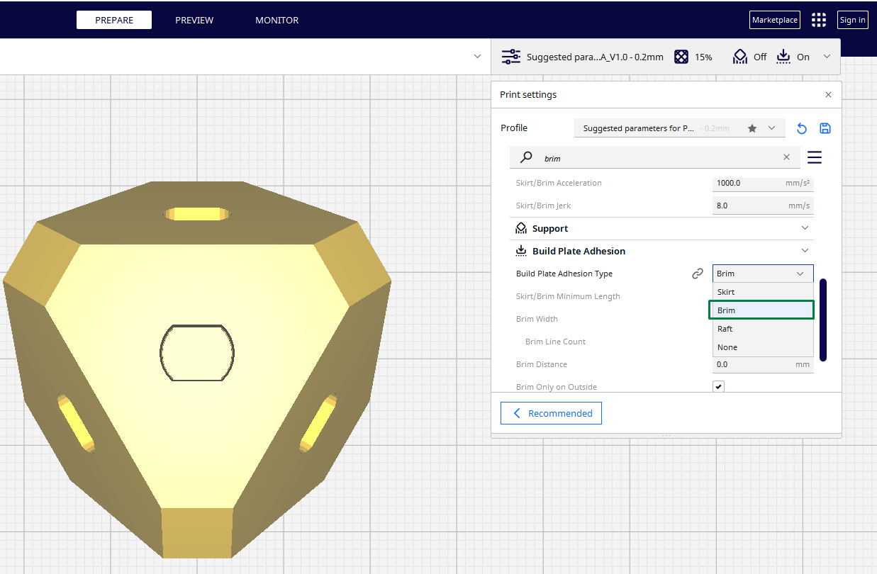
2. Navigate to build plate adhesion from the print settings section and choose Brim.
(Image credit: Tom’s Hardware)
3. Adjust brim settings to customize it further to fit your needs. The following settings are available:
Brim minimum width: This determines the minimum length of the filament that will be used when 3D printing the brim. The default value is always 250mm, and it is always enough.
Brim width: Determine how wide the brim should be in millimeters. A wider brim adheres more to the printer bed.
Brim line count: You choose how many lines of the brim will be printed around the base of the model. This setting also affects the width of the brim.
Brim distance: It determines the horizontal distance between the first layer of the print outline and the first brim line. You should always retain it at 0mm.
Brim only on outside: You can enable this option so that the brim can be printed on the outside of the model to make it easier to remove it after 3D printing, as it reduces the amount to be removed.
Brim inside avoid margin: This setting determines the distance of the brim that will be removed from the outer brim that touches the internal of the other part. You should retain the default value, 2.5mm, and see if it works for your design. If not, you can adjust it.
Smart brim: When you enable it, it improves brim removal by swapping the print order of the innermost and second innermost brim lines.
4. Review and slice: Review all your settings, including the brim settings, and ensure everything is okay before exporting your G-code file after slicing.
How to Achieve a Good 3D Printing Brim
Sometimes your brim might have issues like not correctly sticking to the bed, or even it can be challenging to remove from the print because it is either too thick or too thin. You can consider doing the following to solve those issues.
1. Use Appropriate Brim Settings
(Image credit: Tom’s Hardware)
You can adjust the settings highlighted above until you get the most appropriate one for your 3D prints. For example, you can choose a brim width that provides sufficient adhesion while not being excessive.
If there are adhesion issues, you can consider increasing the brim line count to provide more support by printing more lines around the object. However, you should not add too many as it can make the removal process challenging. Additionally, ensure that the smart brim settings are selected, too, as it makes it easier to remove the brim.
2. Properly Level Your 3D Printer Bed
(Image credit: Tom’s Hardware)
Bed leveling is often the first culprit most of us consider when facing any 3D printer issue, as it plays a crucial role in the quality and success of the first layer. If it isn’t level, some areas might be too close to the nozzle, while other areas might be too far away, leading to poor adhesion or even detachment of the brim. So before you start 3D printing, you should properly level your 3D printer bed.
3. 3D Printer Material You Use
Different materials may require adjustments to brim settings. Materials like ABS are prone to warping and need a wider brim or increased line count for it to be printed well. A wider brim involves adding more lines to the edges of the part to help create a stronger, more stable part. For other materials like PLA, you can lower the brim settings.
4. Use the Correct Temperature
If you are using too high or too low temperatures, it can affect your brim. Too high bed temperatures can cause the brim to adhere too firmly to the build surface, making the removal process more challenging and increasing the risk of damaging the main print when trying to detach it.
Also, high temperatures can cause the filament to be heated much, and become fluid, which can result in the deformation of the brim, causing it to lose its intended shape and compromise the accuracy of the first layers.
If the temperature is too low, it can cause insufficient bed temperatures resulting in weak adhesion between the brim and the build surface. So it’s important to choose the optimal 3D printing temperature for your specific filament to achieve the perfect print.
Venerable shareware archiving app WinRAR has recently been patched to fix an alarming flaw. The update to WinRAR version 6.23, spotted by Bleeping Computer, fixes the vulnerability to the high-severity CVE-2023-40477. In brief, earlier versions of WinRAR were vectors for running a program (arbitrary code execution) if an attacker could tempt the user to open a specially crafted RAR file.
If we look at the Zero Day Initiative’s description of the now-patched WinRAR flaw, it explains the following:
The vulnerability allowed remote attackers to execute arbitrary code,
The flaw was due to the program’s handling of recovery volumes,
The flaw stemmed from the application’s improper validation of user-supplied data,
This meant hackers could access memory beyond the end of an allocated buffer for their dastardly deeds, but…
Importantly, a user would have to visit a disguised malicious page or open a file to fall victim to hackers.
(Image credit: Zero Day Initiative)
Security researcher “goodbyeselene” is credited with discovering the WinRAR flaw described in CVE-2023-40477. They reported the vulnerability to WinRAR developers in early June. News of the flaw was published (August 17) several days after version 6.23 had become available for users to download (August 2), so that people had plenty of time to update.
In the WinRAR v6.23 release notes we see CVE-2023-40477 described as “a security issue involving out of bounds write is fixed in RAR4 recovery volumes processing code.” However, it doesn’t look like it was the only vulnerability squashed, as v6.23 also could be steered to “start a wrong file,” after a user double clicked an item in a specially crafted archive.
Is WinRAR Doomed?
Back in May, we covered the news that Windows would be adding native RAR support in a future update – similar in the way to how it currently handles .zip files. This Windows 11 File Explorer enhancement is delivered thanks to the folding-in of open-source project libarchive. With libarchive integration, Windows should be able to (de)compress many more archives like lha, pax, tar, tgz, and 7z formats. Though devs/testers can dabble with native RAR support now, it is only expected to arrive for mass consumption starting from next month.
WinRAR has put a brave face on the fact that Windows 11 is soon to get integrated support for this popular archiving format. Of course, a Windows integrated RAR archive context menu isn’t going to replace a fully featured app like WinRAR and all its archive processing options.
The explosion of AI is further heightening demand for storage performance and capacity as organizations feed models and databases with unprecedented amounts of data, meaning the next generation of storage technologies will need to deliver even greater performance, density and capacity than ever before.
Supermicro’s fourth annual Open Storage Summit brings together leading storage experts from across the industry including drive manufacturers, compute components manufacturers, software developers and of course Supermicro’s industry leading system architects to discuss the latest in storage technologies and how they will solve tomorrow’s data challenges from the data center right out to the intelligent edge.
This year’s Summit includes a roundtable keynote session followed by five focus sessions, with guests from the storage industry’s leading players including Intel®, AMD, NVIDIA, Micron, Kioxia, Solidigm, and Samsung, as well as Supermicro’s storage software partners.
New Innovations For Storage Performance
(Image credit: Supermicro )
Organizations remain increasingly hungry for ever-more dense data storage systems that satisfy their burgeoning data requirements, but they also need to ensure that such systems remain physically and environmentally stable. Ongoing advancements in flash are providing businesses with new menu items that can help them solve critical business challenges while reducing the total cost of ownership (TCO).
During this kickoff session for the 2023 Open Storage Summit, you will discover how technical advances in flash storage, including the introduction of the E3.S form factor and Compute Express Link (CXL), bring a new evolution to what is already a revolutionary technology. In addition, you’ll also learn how Supermicro is incorporating these new technologies into the latest generation of systems as well as some of the challenges encountered along the way.
During this segment, you will:
Be introduced to new features and improvements in E3.S and learn how they can help transform your business
Get a peek at the future capacity roadmap for flash, including new form factors such as E3.S, the path to even higher drive capacities, and what’s in store for subsequent generations of storage
Discover how storage innovations increase performance and lower TCO
Learn about how CXL can breathe new performance life into critical business applications
Register for upcoming webinars
Join the discussion! Register now for full access to the storage industry’s leading online event to get the latest on key storage trends as well as exclusive look into the future of high performance storage from the most influential minds in the industry.
Register now to get the latest on key storage trends and enter for a chance to win a $250 Amazon gift card.
A research team with the University of California, Berkeley, reconstructed Pink Floyd’s iconic song “Another Brick in the Wall, Part 1” purely by decoding a listener’s brainwaves. Led by Dr. Robert Knight et al. and published in the journal PLOS Biology, the feat showcases how good humanity has become at decoding information that should be the last bulwark of privacy. In the future, someone with access to this technology wouldn’t even have to pay the proverbial penny for your thoughts: they’ll just be able to read them as well as one of those NYU ad walls.
The research, which took place between 2012 and 2013, strapped the brains of 29 epilepsy-suffering patients to electrodes (unlike other approaches, these had to be directly connected to the patient’s brain, meaning invasive surgery was required). The electrodes then captured the electrical activity of brain regions specifically responsible for music processing – areas that focus on pattern recognition and processing of tone, rhythm, harmony, and words.
The researchers then played a 3-minute clip from the original song, and the EEG proved to be accurate enough that they could decode the contents of the patients’ brainwaves – and successfully reconstruct the song from the brain activity’s electrical “echoes.” They even got part of the reconstructed song – 22 seconds – in a sound clip.
Brain-Computer Interfaces (BCI) are one of the most promising research areas for the bodily impaired (with specific applications even for the brain-function impaired segment of the population). But any great advancement presents itself as a double-edged sword. As Orwell’s increasingly-relevant 1984 novel shows, Thinkpol (Newspeak for Thought Police) is one area that any authoritarian regime (or person, or company) would love to explore.
There’s also the risk to the fabric of society. Interpersonal relationships happen in the space that lies between the thoughts we have in private (“Jesus, mom, I hate you for making me eat spinach”) and those we choose to release onto the real world (“But mom, I had spinach yesterday!”). But when the frontier between private and public is blurred, it becomes difficult to understand precisely where chips might ultimately fall – and who might be most negatively impacted.
It’s one thing to be able to reconstruct the outside world (and its stimuli) from a person’s brainwaves, but it’s also a typical truth that research tends to trickle down towards the consumer space (let alone the private and governmental branches of society). While it isn’t in the same league as the research covered in this article, even gamers have taken advantage of brain waves to control their in-game characters. Just look at what Twitter user @perrykaryal managed to do on From Software’s Elden Ring with a “simple” electroencephalogram machine (EEG). I couldn’t beat Godrick with my thumbs; she managed to do it by just thinking about it.
The fact that these experiments required physical contact and invasive surgery precludes most of the “bad actor” threats that could emerge from it. But there shouldn’t be any doubt that, given enough time, techniques that don’t require much physical availability will be developed.
I, for one, would love to be able to simply think articles into existence. But questions must be asked whether the benefits of such a technology being generalized outweigh the risks. Then again, most of us are lucky not to have to deal with life-limiting illnesses such as the epilepsy patients that took voluntary part in the study – it’s almost guaranteed they’d have a different outlook on all of this.
The newer Ryzen 5 5600G (Cezanne) has replaced the Ryzen 5 4600G (Renoir) as one of the best CPUs for gaming. However, a trick has breathed new life into the Ryzen 5 4600G, transforming the budget Zen 2 APU into a 16GB graphics card to run AI applications on Linux.
Not everyone has to budget to buy or rent a Nvidia H100 (Hopper) to experiment with AI. With the current demand for AI-focused graphics cards, you may be unable to access one even if you have the money. Luckily, you don’t need an expensive H100, an A100 (Ampere), or one of the best graphics cards for AI. One Redditor demonstrated how a Ryzen 5 4600G retailing for $95 can tackle different AI workloads.
The Ryzen 5 4600G, which came out in 2020, is a hexa-core, 12-thread APU with Zen 2 cores that operate with a base and boost clock of 3.7 GHz and 4.2 GHz. The 65W chip also wields a Radeon Vega iGPU with seven compute units clocked up to 1.9 GHz. Remember that APUs don’t have dedicated memory but share system memory. You can determine the amount of memory inside the motherboard’s BIOS. In this case, the Redditor had 32GB of DDR4 and allocated 16GB to the Ryzen 5 4600G. Typically, 16GB is the maximum amount of memory you can dedicate to the iGPU. However, some user reports claim that certain ASRock AMD motherboards allow for higher memory allocation, rumored up to 64GB.
The trick converts the Ryzen 5 4600G into a 16GB “graphics card,” flaunting more memory than some of Nvidia’s latest GeForce RTX 40-series SKUs, such as the GeForce RTX 4070 or GeForce RTX 4070 Ti, which are limited to 12GB. Logically, the APU doesn’t deliver the same performance as a high-end graphics card, but at least it won’t run out of memory during AI workloads, as 16GB is plenty for non-serious tasks.
AMD’s Radeon Open Compute platform (ROCm) doesn’t officially support Ryzen APUs. Third-party companies, such as BruhnBruhn Holding, offer experimental packages of ROCm that’ll work with APUs. That means APUs can work with PyTorch and TensorFlow frameworks, opening the gate to most AI software. We wonder if AMD’s latest mobile Ryzen chips, like Phoenix that taps into DDR5 memory, can work and what kind of performance they bring.
The Redditor shared a YouTube video claiming that the Ryzen 5 4600G could run a plethora of AI applications, including Stable Diffusion, FastChat, MiniGPT-4, Alpaca-LoRA, Whisper, LLM, and LLaMA. Unfortunately, he only provided demos for Stable Diffusion, an AI image generator based on text input. He doesn’t detail how he got the Ryzen 5 4600G to work with the AI software on his Linux system. The YouTuber has vouched to release a thorough video of the setup process.
As for the performance, the Ryzen 5 4600G only took around one minute and 50 seconds to generate a 512 x 512-pixel image with the default setting of 50 steps. It’s an excellent result for a $95 APU and rivals some high-end processors. The author said he used DDR4 memory but didn’t list the specifications. Although the Ryzen 5 4600G natively supports DDR4-3200, many samples can hit DDR4-4000, so it would be fascinating to see AI performance scaling with faster memory.
The experiment is fantastic for those who own a Ryzen 5 4600G or Ryzen 5 5600G and want to play around with AI. For those who don’t, throwing $500 into an APU build doesn’t make much sense when you can probably get a discrete graphics card that offers better performance. For instance, AMD’s Radeon 16GB graphics cards start at $499, and Nvidia recently launched the GeForce RTX 4060 Ti 16GB, which has a similar starting price.
Prices for gallium are reported to have increased by 50% in just the past seventeen days, following the August 1st enforcement of China’s export restrictions on the rare metal. A vital yet relatively underrepresented material used in chipmaking (especially when reacted towards gallium arsenide [GaA] and gallium nitride [GaN]), gallium production (like that of many other rare earth metals) lays primarily in China’s hands. The country commands as much as 80% of the world’s output, making it a prime candidate for leverage in the global economic tug-of-war between the U.S. and the Middle Kingdom.
As reported by Bloomberg, the price increase means that gallium now sits at a 10-month-high of $400 per kilogram, putting a deeper squeeze on chipmakers and companies that depend on the material (luckily, in trace amounts) for high-performance semiconductor designs. For perspective, high-purity silicon metal (Si) is currently quoted at an average of $2,000 per metric ton – meaning a kilogram runs chipmakers just $2.
Worldwide, gallium refinement facilities are primarily present throughout China and Japan. A lone facility also exists in Europe, but as expected, that’s not nearly enough for the continent’s needs, let alone as an alternative source for the globalized (yet restricted) market. Therefore, non-producing countries must import either the base metal or already-processed gallium arsenide wafers.
Yet due to China’s imposed restrictions, U.S.-based entities looking to import the metal must submit for registration with China’s Ministry of Commerce. While that is a relatively common requirement, the fact that companies could only apply for a license starting August 1st (the same day the export restrictions went into effect) creates a measure of attrition. Add to that the fact that obtaining the license can take up to 45 days and that China announced the restrictions with barely a month to go for companies to adjust (in early July), and the stage was set for the country’s intended disruption.
Due to its relatively exotic usage in electronics and semiconductors, a squeeze on the supply side of gallium disproportionally impacts the U.S.’s chipmaking capabilities. While China may be its home at extraction, the country’s 5-generation gap compared to the U.S. in leading-edge microelectronics means there aren’t many occasions for its chipmaking players to take advantage of its properties. At the same time, the export restrictions mean that China can start stockpiling the rare metal for deployment whenever its chip manufacturing processes are up to the task.
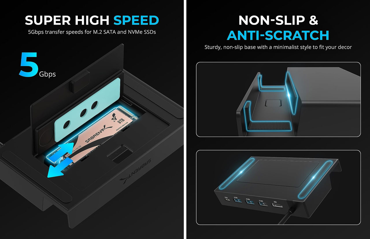
Sabrent has released a refined and expanded update to its first Steam Deck Dock (the DS-SD6P) in the shape of the new DS-SDNV, available now on Amazon. Also described as the ‘Sabrent 7-in-1 Steam Deck Dock with M.2 SSD Slot’, this device packs quite a lot of features into a familiar-looking device stand form-factor.
The Sabrent DS-SDNV isn’t restricted to use with the Steam Deck. It is claimed to be equally happy docking with a ROG Ally or other USB Type-C devices with DisplayPort Alternate (DP Alt) Mode support for output through HDMI 2.0 (HDCP 1.4). Linux, Windows, and macOS are supported.
If you have a compatible device/OS, there is quite a lot of convenient expandability offered here. The following ports are all easily accessible on this USB-C dock:
HDMI 2.0
USB 2.0
Two USB 3.2
USB Type-C PD 3.0
Gigabit Ethernet RJ45
(Image credit: Sabrent)
The slower USB port might be ideal for a mouse/keyboard, while the faster ports can be used for data transfer or other high-speed peripheral usage. Having a wired gigabit network port might also be appealing, with typically improved reliability, speed, and latency compared to wireless connectivity.
Moving on to what might be the Sabrent DS-SDNV’s raison d’être – it can fit an M.2 SSD inside. Under the device’s base, users can remove a cover panel and fit in their choice of M.2 drive. It looks like it can accept any size drive up to 80mm in length (M.2 2280), and Sabrent shows it with a roomy 8TB in place.
(Image credit: Sabrent)
The dock’s M.2 slot is equally happy with an M.2 SATA or NVMe drive. Its quoted maximum speed is 5 Gbps, so it sounds like there would be no speed advantage offered by the NVMe option here. If you need more storage and must keep it portable and as fast as possible, you may be better off replacing the Steam Deck’s internal M.2 2230 SSD.
Finally, Sabrent has some words about its dock’s build quality. It says it is rugged, yet minimalist to blend in with your décor. Additionally, non-slip anti-scratch pads are present on the device’s base, and within its docking cradle.
The Sabrent 7-in-1 Steam Deck Dock with M.2 SSD Slot DS-SDNV is currently listed at $84 on Amazon, with four in stock. That’s a lot more expensive than the first Sabrent Steam Deck Dock was pitched at (with no M.2 slot). However, it is roughly the same price as the official Valve Steam Deck Dock, which we thought was both uninspiring and a poor value.
The chief executive of SMIC faced criticism for proposing to advance chip packaging technologies and multi-chiplet designs after the company lost access to 7nm and 10nm-capable wafer fab tools due to U.S. sanctions. But his vision has now become central to China’s semiconductor approach for 2023, according to DigiTimes. Industry heavyweights like Huawei and government-backed entities with deep pockets are making substantial progress in this domain. Companies like JCET and Tongfu already offer their clients 2.5D and 3D packaging technologies.
Through the National Natural Science Foundation of China (NSFC), the Chinese government is channeling more funds into chiplet research. NSFC’s 2023 research areas encompass advanced 2.5D/3D packaging techniques, reusable chiplet design methods, parallel processing for multiple chiplets, electronic design automation (EDA) tools, and comprehensive multi-chiplet simulations. This intensified focus on chiplet technology showcases China’s strategy to minimize its dependence on foreign semiconductor innovations.
Large companies are also making strides in chiplet design, packaging, and multi-chiplet technologies. For example, Huawei ramped up chiplet-related patent filings from 30 in 2017 to over 900 in 2022. China-based companies recently formed the China Chiplet League to advance the homegrown Chiplet Interconnect Interface Standard.
Chinese companies are by no means novices in advanced packaging. Yet, for now, most of their efforts are tailored to cater to demand from non-Chinese companies with access to Taiwan-based TSMC and ASE Technology Group, the world’s largest outsourced semiconductor assembly and test (OSAT) company.
JCET, the world’s third-largest OSAT, is involved in the chiplet sector. The company can package chiplets made on a 4nm-class process technology, which is nearly on par with what TSMC can offer and is good enough to cater to domestic and international clientele.
Tongfu, another top OSAT, also has developed a set of 2.5D, 3D, and advanced chiplet packaging technologies. Tongfu reportedly indicated that it anticipates continuing benefits from AMD’s broad adoption of chiplet technology in the future. This suggests Tongfu has aligned its technological advancements with industry trends and foresees potential collaborations or synergies with major players like AMD.
NationalChip is collaborating on high-performance interconnect IP designs for chiplet applications. The company is also researching advanced chip design, including high-bandwidth memory (HBM) technology, with a primary focus on creating tailored products for customers.
As for VeriSilicon, it has multiple verification tools for multi-chiplet designs that are reportedly used by companies serving the high-performance computing (HPC) sector.
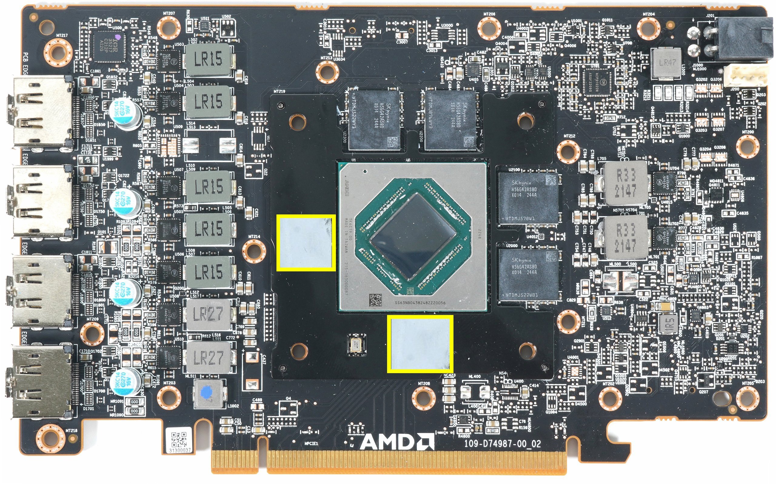
AMD has encountered some unfortunate issues with mounting pressure on some of its Best GPUs in the past. However, a new report from Igor’s Lab discovered a similar problem with AMD’s new Radeon Pro W7600 single-slot graphics card that is much worse, leading to complete blackouts from the GPU.
The symptoms began when Igor tested AMD’s new single-slot W7600 for a review. He found that testing the card for less than 6 minutes under Lightwave, Horizon Zero Dawn or Furmark would cause the GPU to stop producing an image to the monitor altogether — causing the screen to blackout. This happened even though the card’s PCB, memory, and GPU temperatures were being reported within their specified limits (albeit at the higher end of those limits).
It turns out there was a serious problem with the thermal pads AMD installed on the Radeon Pro W7600. Igor discovered that the thermal pads covering the four GDDR6 memory modules were too thick and too hard, resulting in the single-slot vapor camber tilting on the GPU die and preventing the GPU die from making perfect contact with the vapor chamber cooler.
To make matters worse, AMD did not add additional spacers to the W7600 to counter the mounting pressure from the extra-thick memory pads. The W7600’s four GDDR6 memory modules sit right next to the GPU die, on the top and right sides, forcing all the contact pressure from the pads to sit on one side of the card. Spacers are a common practice in the consumer GPU space to ensure that GPU mounting pressure remains sufficient across all die areas.
AMD also did not provide direct contact from the heatsink to the W7600’s mid-plate sandwiched between the PCB and the cooler. Doing this traps heat in and around the memory modules since they and their associated thermal pads are directly connected to the mid-plate.
You’re supposed to make cutouts for the GDDR6 memory modules so that the thermal pads can directly contact the cooler, bypassing the mid-plate altogether. Or, you connect the mid-plate to the cooler with thermal pads or a combination of thermally conductive metals paired with thermal pads.
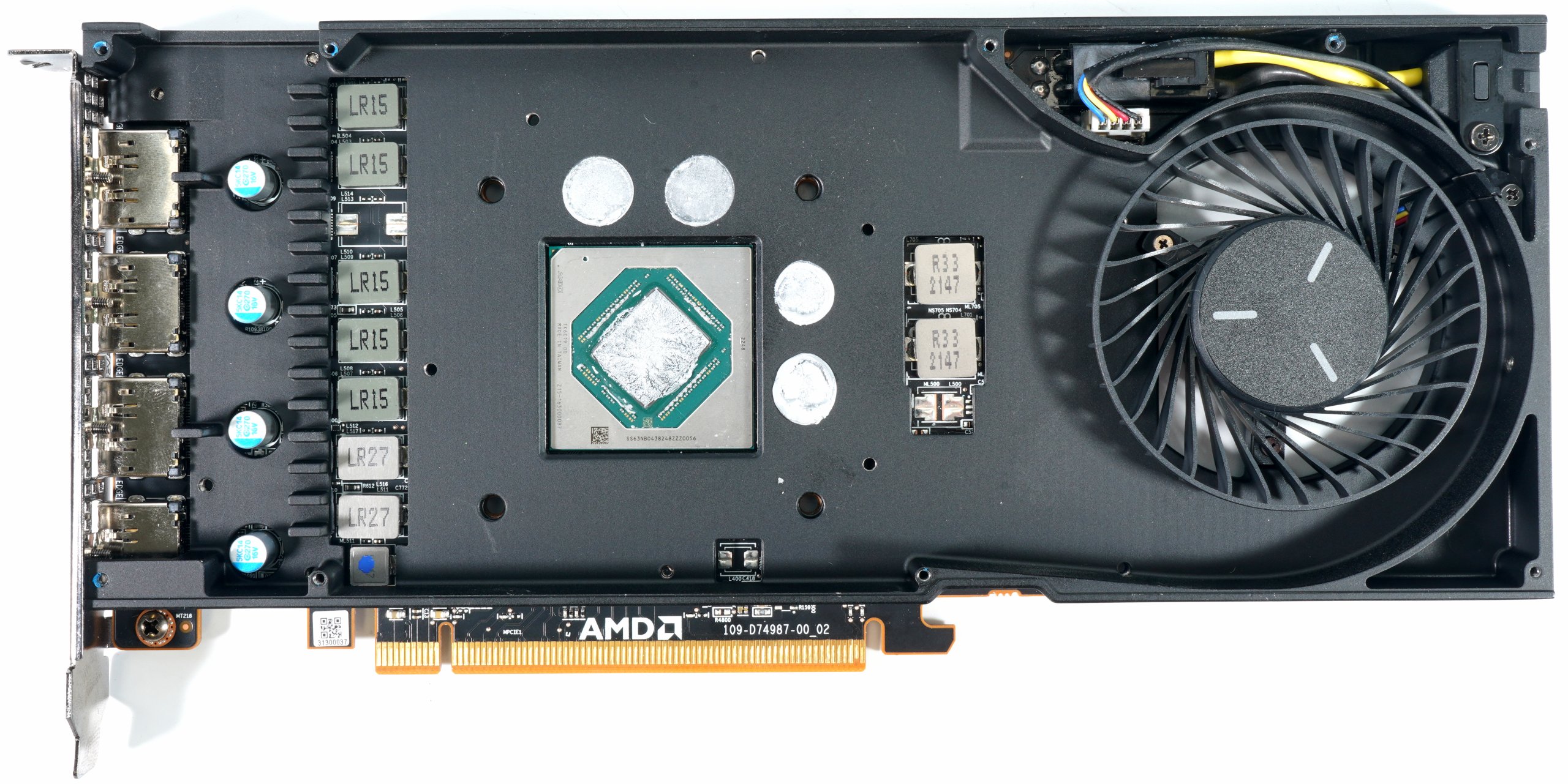
Igor’s W7600 Thermal Paste Modification For The Mid-Plate (Image credit: Igor’s Lab)
To fix the issue, all Igor did was replace the GDDR6 memory pads with slightly thinner and softer 0.5mm pads to reduce the right and top-most mounting pressure, apply two additional pads on the opposite sides of the GDDR6 memory modules to stabilize the cooler, and use additional thermal paste connecting the heatsink to the mid-plate. As a result, the mid-plate now has direct contact with the heatsink, allowing all the heat generated from the memory ICs to be transferred directly into the heatsink.
It’s surprising to see such mediocre craftsmanship from AMD, especially on a card designed for the workstation market. Usually, workstation cards are held to higher manufacturing standards than gaming cards due to their purpose. But this isn’t the first time we’ve seen cooling problems like this from AMD. A similar issue was also present on AMD’s reference RX 7900 XTX graphics card, which caused GPU hotspot temps to spike as high as 110C even though the GPU core might be sitting as low as 50-60C.
For now, Igor seems to be the only one with this issue, but we do not doubt that more people will have similar issues down the road as the card ages. Hopefully, AMD will rectify the problem quickly with another revision of the Pro W7600 in the near future.